Method for manufacturing TSV seed layer with fine pitch and high depth-to-width ratio

A manufacturing method and high aspect ratio technology, applied in the field of microelectronics, can solve problems such as sealing the TSV mouth, and achieve the effect of low cost and easy realization

Inactive Publication Date: 2013-10-09
NAT CENT FOR ADVANCED PACKAGING
View PDF4 Cites 5 Cited by
  • Summary
  • Abstract
  • Description
  • Claims
  • Application Information

AI Technical Summary

Problems solved by technology

[0005] In view of the above-mentioned problem of TSV mouth sealing that is easy to occur during the deposition process of the seed layer when the TSV aperture is small, the present invention provides a method for manufacturing the seed layer that combines copper reflow, plasma enhancement technology and PVD technology

Method used


Image

  • Method for manufacturing TSV seed layer with fine pitch and high depth-to-width ratio
  • Method for manufacturing TSV seed layer with fine pitch and high depth-to-width ratio
  • Method for manufacturing TSV seed layer with fine pitch and high depth-to-width ratio

Examples


Embodiment Construction

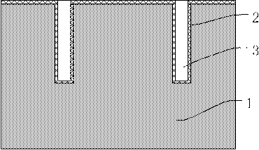
[0025] figure 1 Shown is the wafer substrate that has completed the TSV etching and insulating layer deposition process, where 1 is the substrate and 2 is the barrier layer. The film layer can be silicon dioxide, silicon nitride, silicon oxynitride, organic polymer materials etc. 3 is a TSV hole. There can be zero or more layers of membrane structure 2 covering the sidewall of the deep hole as required.

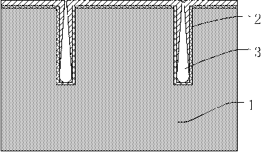
[0026] A metal layer 4 is deposited on the surface of the substrate 1 and in the TSV hole 3 by using a PVD process, such as figure 2 shown. The PVD metal layer includes a barrier layer adhesion layer metal and a seed layer. The material of the barrier layer adhesion layer can be titanium, titanium nitride, tantalum, tantalum nitride, tungsten, tungsten nitride, vanadium, single vanadium, niobium, nitrogen Niobium chloride, etc., and the material of the seed layer is copper.

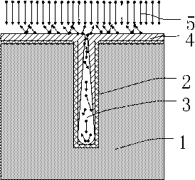
[0027] After the copper is deposited by PVD, the wafer is heated and reflowed in a vacuum or lo...


PUM


Abstract

The invention relates to a method for manufacturing a TSV seed layer with a fine pitch and a high depth-to-width ratio, belongs to the microelectronic processing technology, and aims to solve the problem that when the bore diameter of a TSV is approximate to or even less than 1 micron, a target material in a PVD process can easily seal an opening of the TSV so that the target material cannot enter the TSV. According to the method, after the PVD is utilized for finishing the deposition of the seed layer, a wafer is placed in a vacuum or low-pressure environment for heating reflux, so that the mobility of a copper seed layer is enhanced; meanwhile, plasma bombard is conducted as a supplement to boost the copper seed layer to flow towards the lower middle portion of the TSV, and the seed layer on the opening of the TSV can be splashed back at the same time to enable the opening of the TSV to be opened. The process of depositing the copper seed layer is continued, and then the reflux process and the plasma treatment process are repeated to improve the continuity of the copper seed layer inside the TSV. Therefore, the proceeding of a follow-up electroplating process is facilitated, and the filling effect of the TSV is guaranteed.

Description

technical field [0001] The invention relates to a method for manufacturing or processing semiconductor or solid devices in the technical field of microelectronics, in particular to a method for manufacturing a TSV seed layer with fine pitch and high aspect ratio in the microelectronic processing technology. Background technique [0002] As the feature size of semiconductor chips continues to shrink following Moore's Law, the performance of semiconductor devices continues to improve, but at the same time, interconnection performance continues to deteriorate due to the reduction of line width, making interconnection lines gradually become a limit to the performance of semiconductor chips. the bottleneck. Through-silicon vias or through-silicon vias (Through Silicon Via, TSV) effectively use the third dimension of semiconductor chips, which can make up for the limitations of traditional semiconductor chips with only two-dimensional wiring, and are an important way to solve the ...

Claims


Application Information

Patent Timeline
Patent Type & Authority Applications(China)
IPC IPC(8): H01L21/768
Inventor 薛恺于大全
Owner NAT CENT FOR ADVANCED PACKAGING
Why Eureka
Try Eureka