Dual-photoresist and processing method thereof

A processing method and photoresist technology, applied in the direction of microlithography exposure equipment, optics, optomechanical equipment, etc., can solve the problems of low etching selection and poor fidelity of pattern transfer, and achieve pattern accuracy, light reduction, etc. Effect of small loss of fidelity

Active Publication Date: 2013-10-23
SEMICON MFG INT (SHANGHAI) CORP
View PDF5 Cites 7 Cited by
  • Summary
  • Abstract
  • Description
  • Claims
  • Application Information

AI Technical Summary

Problems solved by technology

However, in the process of transferring the upper layer pattern to the lower layer photoresist by etching, the fidelity of the pattern transfer is not very good. One of the important reasons is that the positive and negative photoresists generally used are all made of carbon atoms. As the main component of the material, the selection of etching is relatively low, which leads to the problem of pattern size and side verticality caused by etching

Method used


Image

  • Dual-photoresist and processing method thereof
  • Dual-photoresist and processing method thereof
  • Dual-photoresist and processing method thereof

Examples


Embodiment 1

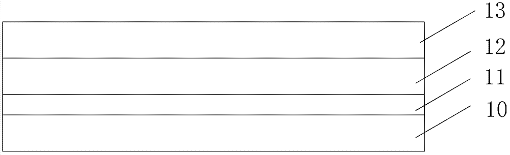
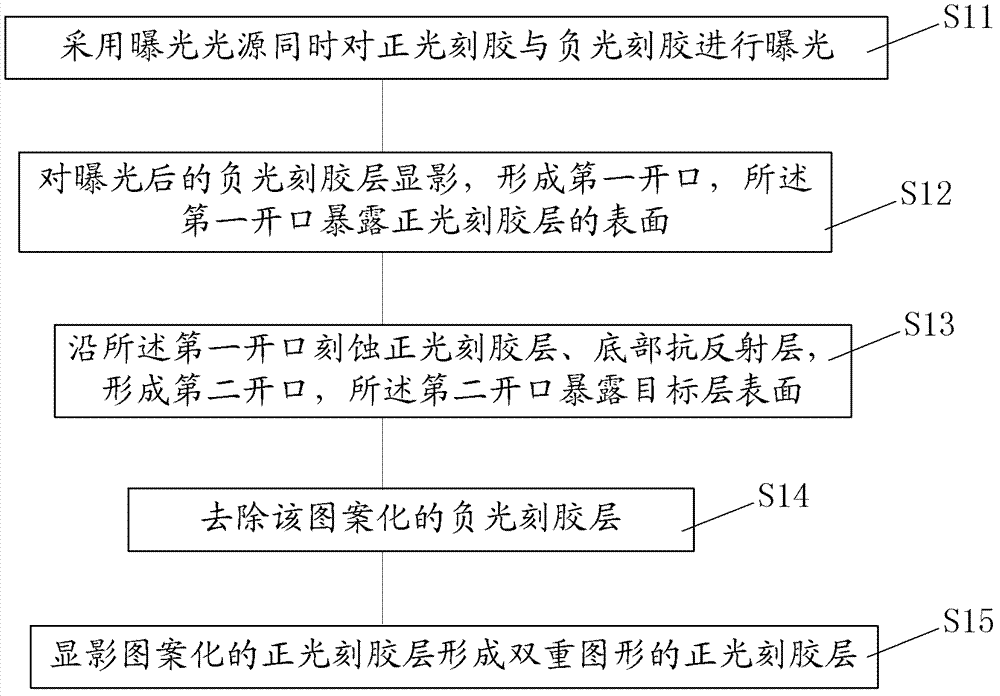
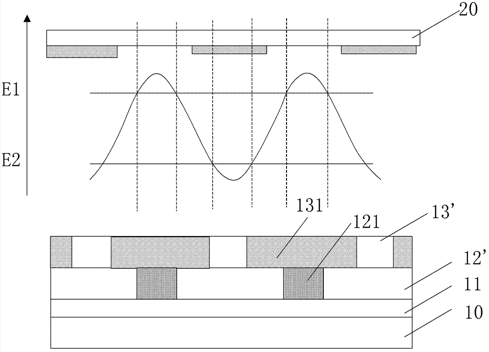
[0037] refer tofigure 1 As shown, the double photoresist provided in the first embodiment is formed on the target layer 10 , which are bottom antireflection layer (BARC) 11 , positive photoresist layer 12 and negative photoresist layer 13 in sequence from bottom to top. The bottom anti-reflection layer 11 is used to increase the intensity of bottom light in the exposure process, and the material can be selected from existing BARC materials, and can be an organic anti-reflection coating or an inorganic anti-reflection coating.

[0038] The inorganic antireflection coating is made of, for example, titanium (titanium), titanium oxide (titanium oxide), titanium nitride (titanium nitride), chromium oxide (chromium oxide), carbon (carbon), amorphous silicon (amorphous silicon), nitrogen Silicon nitride (silicon nitride), silicon nitride oxide (silicon nitride oxide), silicon carbon oxide (silicon carbon oxide) and other materials; the organic anti-reflection coating is made of, for e...

Embodiment 2

[0061] The structure and processing method of the double photoresist provided in the second embodiment and the first embodiment are roughly the same, the only difference is that the double photoresist on the target layer 10 is sequentially from bottom to top: bottom anti-reflection layer (BARC) 11. Negative photoresist layer and silicon-containing water-soluble positive photoresist layer. Wherein, the material selection of each layer of the negative photoresist layer and the silicon-containing water-soluble positive photoresist layer is the same as that of the first embodiment. The bottom anti-reflection layer 11 is an optional layer, which is used to increase the intensity of bottom light in the exposure process, and the material can be selected from existing BARC materials.

[0062] Aiming at the differences between the second embodiment and the first embodiment, the method for processing the double photoresist in the second embodiment will be briefly introduced below. Firs...


PUM

PropertyMeasurementUnit
thicknessaaaaaaaaaa

Abstract

The invention discloses a dual-photoresist. The dual-photoresist comprises a first photoresist layer and a second photoresist layer which are sequentially formed on a target layer, wherein the first photoresist layer is a positive photoresist layer or a negative photoresist layer, and the polarity of the second photoresist layer is opposite to that of the first photoresist layer, and the first photoresist layer and the second photoresist layer are exposed in a same exposure process; the positive photoresist layer adopts a silicon-containing water-soluble positive photoresist. The invention further provides a processing method of the dual-photoresist. By adopting the technical scheme and adopting the fluorine-containing corrosion gas with high selection ratio to the silicon-containing water-soluble positive photoresist, the transferring between patterns of the dual photoresists is precise, and the controllability of the process is improved.

Description

technical field [0001] The invention relates to the field of semiconductor manufacturing, in particular to a double photoresist and a processing method thereof. Background technique [0002] Generally speaking, a semiconductor device such as a dynamic random access memory (DRAM) includes a large number of fine patterns, which are formed by transferring a mask pattern to a semiconductor layer through photolithography and etching processes. The process of photolithography is generally as follows: coating photoresist (PR) on the target layer to be patterned, then performing an exposure process to change the solubility of the photoresist in some areas, and then performing a development process to form a pattern that exposes the target layer. The photoresist pattern, the above process completes the transfer of the mask pattern to the photoresist. An etching process is performed using the photoresist pattern as a mask to transfer the photoresist pattern onto the semiconductor lay...

Claims


Application Information

Patent Timeline
Patent Type & Authority Applications(China)
IPC IPC(8): G03F7/075G03F7/20
Inventor 胡华勇
Owner SEMICON MFG INT (SHANGHAI) CORP
Why Eureka
Try Eureka