

Preparation method of la-based high dielectric constant gate dielectric material based on germanium substrate
A technology with high dielectric constant and gate dielectric, which is applied in the manufacture of circuits, electrical components, semiconductors/solid-state devices, etc., can solve the problems of poor surface roughness, unfavorable performance, and small equivalent oxide layer of gate dielectrics, and achieve the goal of suppressing Effects of desorption and volatilization, improvement of surface roughness, and improvement of radiation resistance
- Summary
- Abstract
- Description
- Claims
- Application Information
AI Technical Summary
Problems solved by technology
Method used
Image

Examples
example 1
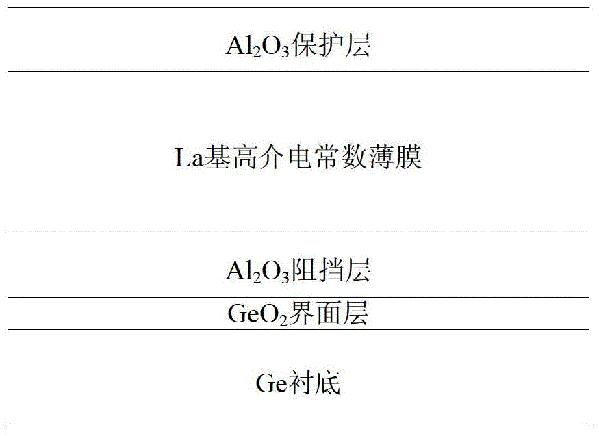
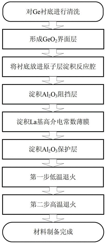
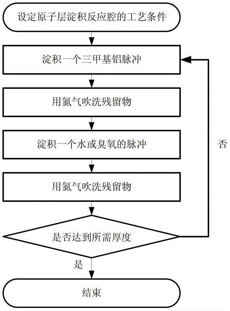
[0056] Example 1, preparation of Al 2 o 3 \La 2 o 3 \Al 2 o 3 \GeO 2 \Ge high dielectric constant gate dielectric material
[0057] Step 1, cleaning the Ge substrate.
[0058] 1a) Clean the Ge substrate in an SC-1 solution heated to 75°C for 10 minutes. The composition of the solution is NH 4 OH, H 2 o 2 and H 2 O, its ratio is 5:1:1, the main effect of this cleaning is to rely on NH 4 Complexation of OH with H 2 o 2 Strong oxidizing ability to remove organic pollutants or attached particles on Ge wafers;
[0059] 1b) Rinse the Ge sheet after cleaning in the SC-1 solution in deionized water for 2 minutes to remove the residual SC-1 solution;
[0060] 1c) Wash the Ge chip in HF solution for 60 seconds, the composition of the solution is HF and H 2 O, whose ratio is 1:400, the main function of this cleaning is to remove the natural oxide layer GeO on the surface of the Ge substrate. 2 ;
[0061] 1d) rinsing the Ge sheet from which the natural oxide layer on the ...
example 2
[0091] Example 2, preparation of Al 2 o 3 \LaAlO 3 \Al 2 o 3 \GeO 2 \Ge high dielectric constant gate dielectric material
[0092] Step 1, cleaning the Ge substrate.
[0093] 1.1) Clean the Ge chip in the SC-1 solution heated to 75°C for 10 minutes. The composition of the solution is NH 4 OH, H 2 o 2 and H 2 O, its ratio is 5:1:1, the main effect of this cleaning is to rely on NH 4 Complexation of OH with H 2 o 2 Strong oxidizing ability to remove organic pollutants or attached particles on Ge wafers;
[0094] 1.2) Rinse the Ge sheet after cleaning in the SC-1 solution in deionized water for 2 minutes to remove the residual SC-1 solution;
[0095] 1.3) Wash the Ge chip in HF solution for 60 seconds, the composition of the solution is HF and H 2 O, whose ratio is 1:400, the main function of this cleaning is to remove the natural oxide layer GeO on the surface of the Ge substrate. 2 ;
[0096] 1.4) Rinse the Ge sheet in deionized water to remove residual HF solut...
example 3
[0128] Example 3, preparation of Al 2 o 3 \HfLaO\Al 2 o 3 \GeO 2 \Ge high dielectric constant gate dielectric material
[0129] Step A, cleaning the Ge substrate.
[0130] Clean the Ge sheet in an SC-1 solution heated to a temperature of 75°C for 10 minutes to remove organic pollutants or attached particles on the Ge sheet. The composition of the solution is NH 4 OH, H 2 o 2 and H 2 O, the ratio is 5:1:1; then rinse the Ge sheet in deionized water for 2 minutes in SC-1 solution to remove residual SC-1 solution; then wash the Ge sheet in HF and H 2 O ratio is 1:400 in the HF solution cleaning 60 seconds, to remove the natural oxide layer of Ge substrate surface; The Ge plate that removes the natural oxide layer of Ge substrate surface is rinsed in deionized water again, to remove residual HF Solution; put the Ge sheet that removes the residual HF solution into deionized water and use ultrasonic cleaning for 5 minutes to remove the adsorption particles on the surface, a...
PUM
| Property | Measurement | Unit |
|---|---|---|
| thickness | aaaaa | aaaaa |
| thickness | aaaaa | aaaaa |
| thickness | aaaaa | aaaaa |
Abstract
Description
Claims
Application Information