Method for preparing gate silicon oxide layers and method for processing semiconductor substrate

A technology of gate silicon oxide and processing method, which is applied in the direction of semiconductor devices, semiconductor/solid-state device manufacturing, electrical components, etc., can solve the problems of affecting channel carrier mobility, complicated process, and reducing carrier mobility, etc. Achieve the effects of surface property optimization, process simplification, and reliability improvement

Inactive Publication Date: 2013-11-13
SEMICON MFG INT (SHANGHAI) CORP
View PDF5 Cites 5 Cited by
  • Summary
  • Abstract
  • Description
  • Claims
  • Application Information

AI Technical Summary

Problems solved by technology

However, in the current process, the peak of the nitrogen concentration distribution is always close to the interface between the gate silicon oxide layer and the substrate silicon, rather than the ideal distribution described above, such a distribution will reduce the mobility of carriers in the channel Rate
However, the commonly used double gate oxide process now generally grows the thick gate silicon oxide 104 and the first thin gate silicon oxide 103 in the high-voltage device regions II and III, and then grows the second thin gate silicon oxide in the low-voltage device region I. 102 (the thickness of the second thin gate silicon oxide 102 is relativel...

Method used


Image

  • Method for preparing gate silicon oxide layers and method for processing semiconductor substrate
  • Method for preparing gate silicon oxide layers and method for processing semiconductor substrate
  • Method for preparing gate silicon oxide layers and method for processing semiconductor substrate

Examples


Embodiment 1

[0042] Such as figure 2 As shown, this implementation provides a method for preparing a gate silicon oxide layer, comprising the following steps:

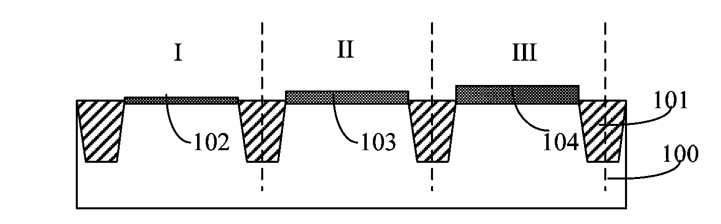
[0043] S21, providing a silicon substrate, forming a device isolation structure in the silicon substrate to isolate the low-voltage device region and the high-voltage device region;

[0044] S22, forming a pad oxide layer on the silicon substrate;

[0045] S23, performing well ion implantation and annealing in the silicon substrate;

[0046] S24, etching the pad oxide layer to expose the channel region of the low-voltage device region and the high-voltage device region;

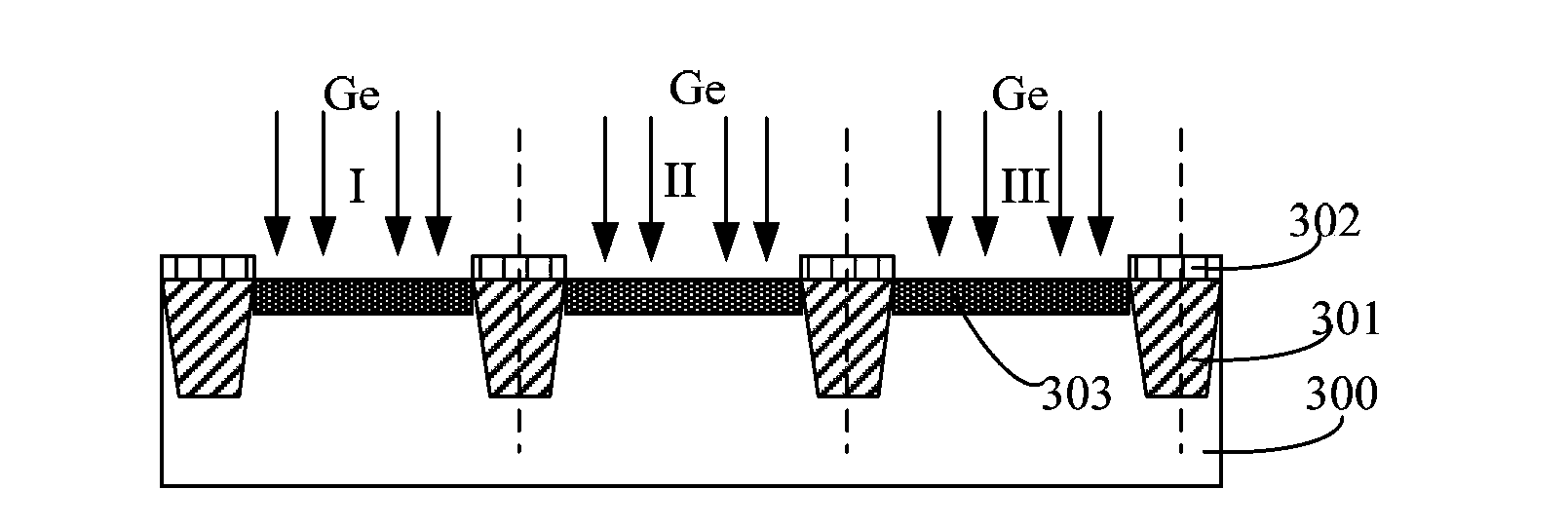
[0047] S25, performing pre-amorphization implantation of germanium ions on the surface of the semiconductor substrate in the low-voltage device region and the high-voltage device region;

[0048] S26, performing nitrogen ion implantation on the surface of the semiconductor substrate in the low-voltage device region, and performing fluorine ion implantation on ...

Embodiment 2

[0065] Such as Figure 4 As shown, this implementation provides a method for preparing a gate silicon oxide layer, comprising the following steps:

[0066] S41, providing a silicon substrate, forming a device isolation structure in the silicon substrate to isolate a low-voltage device region and a high-voltage device region;

[0067] S42, forming a pad oxide layer on the silicon substrate;

[0068] S43, performing well ion implantation and annealing in the silicon substrate;

[0069] S44, performing pre-amorphization implantation of germanium ions on the surface of the semiconductor substrate in the low-voltage device region and the high-voltage device region;

[0070] S45, performing nitrogen ion implantation on the surface of the semiconductor substrate in the low-voltage device region, and performing fluorine ion implantation on the surface of the semiconductor substrate in the high-voltage device region;

[0071] S46, etching the pad oxide layer to expose the channel re...

Embodiment 3

[0087] Such as Figure 7 As shown, the present embodiment provides a method for processing a semiconductor substrate, comprising the following steps:

[0088] S71, providing a semiconductor substrate, where the semiconductor substrate includes a plurality of subregions;

[0089] S72, perform nitrogen ion implantation on the surface of one subregion of the semiconductor substrate, and perform fluorine ion implantation on the surface of another subregion of the semiconductor substrate;

[0090] S73. Thermally oxidize the surface of the semiconductor substrate to grow an oxide layer, and the oxide layer in the sub-region implanted with fluorine ions is thicker than the sub-region implanted with nitrogen ions.

[0091] The semiconductor substrate provided in step S71 includes a plurality of sub-regions, and these sub-regions may be the high-voltage device region and the low-voltage device region described in Embodiment 1 and Embodiment 2, or may be device isolation trenches.

[...


PUM


Abstract

The invention provides a method for preparing gate silicon oxide layers and a method for processing a semiconductor substrate. Nitrogen ions are injected into a low-pressure device area in advance and fluorine ions are injected in a high-pressure device area in advance, so that when the gate silicon oxide layers grow on the surface of the thermal oxidation semiconductor substrate, growth of the gate silicon oxide layers in the low-pressure device area is restrained, growth of the gate silicon oxide layers in the high-pressure device area is promoted, therefore, the gate silicon oxide layers with different thicknesses are formed, and the technological process is greatly simplified; further germanium and/or silicon is injected into the semiconductor substrate in a pre-non-crystallizing mode, and the channel carrier mobility is improved; in the annealing recrystallization process after non-crystallizing injection and nitrogen and fluoride ion injection, the characteristics of the surface of the silicon substrate are optimized, and the method is beneficial to improving the reliability of the gate oxide layers. The fabrication processing enables the peak value of the nitrogen concentration distribution of the low-pressure device area to be close to the surfaces of the gate silicon oxide layers, the follow-up boron penetration from P+ polycrystalline silicon can be effectively blocked, and the reliability of the thin gate silicon oxide layers in the low-pressure device area can be enhanced.

Description

technical field [0001] The invention relates to the field of semiconductor manufacturing, in particular to a method for preparing a gate silicon oxide layer and a method for processing a semiconductor substrate. Background technique [0002] With the rapid development of the microelectronics industry and ultra-large-scale integrated circuits (ULSI), the dual gate oxide process (Dual Gate Oxide, DGO) integrates high-voltage devices and low-voltage devices on the same chip, which is a breakthrough in the deep submicron integrated circuit manufacturing process The key process technology directly affects and determines the electrical characteristics and reliability of the device. It needs to grow gate silicon oxide layers of two thicknesses on the same chip at the same time to prepare transistors working at different voltages. [0003] Such as figure 1 As shown, in the prior art, in a CMOS high-voltage integrated circuit (High-Voltage Integrated Circuits, HVIC) compatible with...

Claims


Application Information

Patent Timeline
IPC IPC(8): H01L21/28H01L21/265
Inventor 赵猛
Owner SEMICON MFG INT (SHANGHAI) CORP
Why Eureka
Try Eureka