Method for improving gap filling capability

A technology for filling capacity and voids, which is applied in the field of semiconductor device manufacturing, can solve problems such as reduced filling capacity, affecting CONT filling, and shorting of CONT, and achieves the effect of reducing aspect ratio and enhancing void filling capacity

Inactive Publication Date: 2013-12-04
HEJIAN TECH SUZHOU
View PDF4 Cites 0 Cited by
  • Summary
  • Abstract
  • Description
  • Claims
  • Application Information

AI Technical Summary

Problems solved by technology

[0002] In the semiconductor method, the component size of the integrated circuit is required to be smaller and smaller, so that more components can be accommodated on a semiconductor chip. As the circuit edge becomes smaller and faster, the distance between the components is also getting smaller and smaller. Based on the special requirements of electrical breakdown, a wider spacer is required as a barrier layer. However, due to the small line width characteristics of the semiconductor method, the width of the barrier layer will make the spacing between Poly narrower, and Its depth will not change because of these, which leads to a large depth-to-width ratio between Polys, resulting in a reduction in the subsequent filling capacity. In the subsequent filling, pores are easy to be generated, and the existence of these pores will directly affect the follow-up. CONT filling, the pores generated during the filling will diffuse when the CONT is filled, which will cause a short circuit between the CONTs, causing the device to fail to work
[0003] In traditional methods, such as Figure 1a , 1b, 1c, 1d, the width of the spacer 1 is fixed after the etch dwell time, although some implant layer (implant layer) acid baths will be passed later, but these photoresist removal steps have no effect on the etching of the oxide layer. The rate is low, and basically has no effect on the width of the spacer. The spacer produced in this way has a large aspect ratio (such as Figure 1a shown), which will cause a reduction in the subsequent filling capacity (for example: ILD filling), and will form pores between fillers (for example: ILD) (such as Figure 1b shown)
The existence of void (void) 3 will form a conduction channel in the circuit, and in the subsequent CONT tungsten filling process, metal tungsten will be filled into the channel connected by the void (such as Figure 1d shown), resulting in a short circuit of the circuit, causing fatal damage to the device

Method used


Image

  • Method for improving gap filling capability
  • Method for improving gap filling capability
  • Method for improving gap filling capability

Examples


Embodiment 1

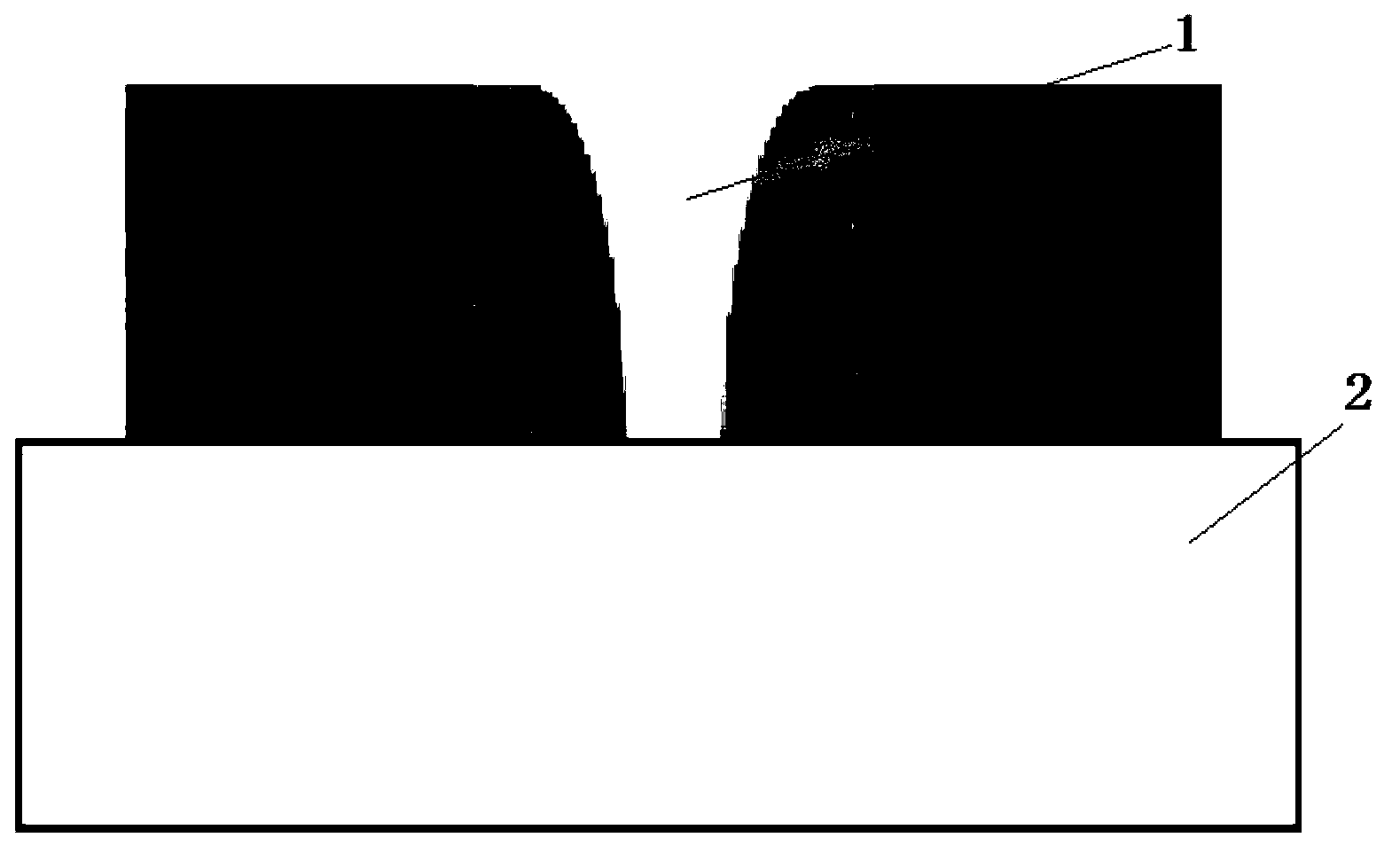
[0036] As shown in Figures 1 and 2, a method for improving the gap filling capability includes the following steps: Step 1: Forming a spacer 1 with a certain aspect ratio on the ONO structure by etching; Step 2: Using DHF to form a spacer 1 1. Carry out secondary etching, DHF etching residence time is determined according to the needs of different methods, and reduce the aspect ratio of the spacer; Step 3: Fill the spacer with ILD; Step 4: Carry out metal tungsten film growth. Among them, the ONO structure is a silicon oxide-silicon nitride-silicon oxide layer, and the formation method is chemical vapor deposition (VCD).

[0037] In this embodiment, compared with the traditional method, an acid tank etching process is added. Since DHF has a high ET (residence time) selectivity ratio for the oxide layer, after DHF acid tank etching, the width of the upper part of the spacer is enlarged. , thereby enlarging the filling window of the ILD, reducing the aspect ratio of the spacer, ...

Embodiment 2

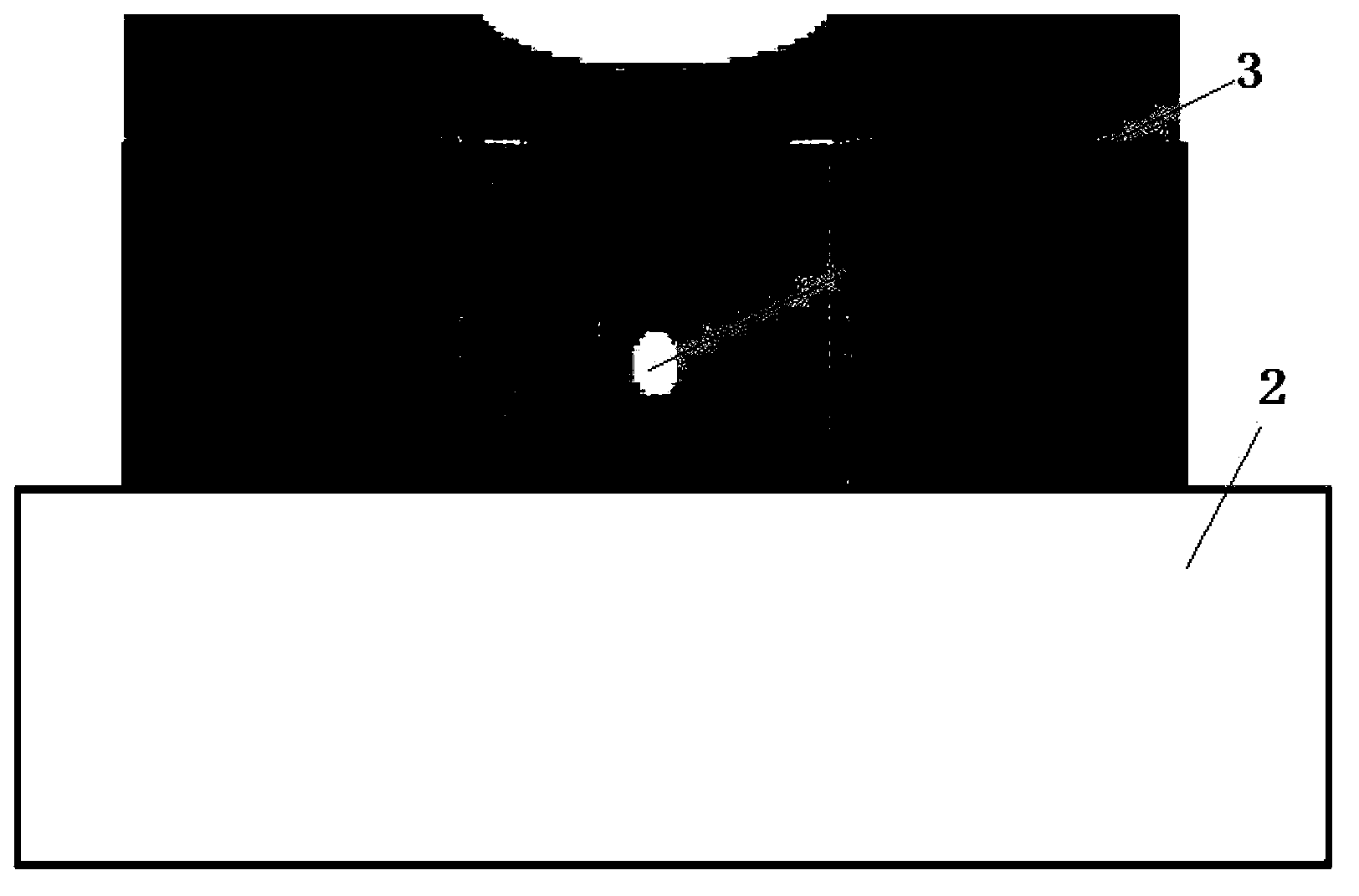
[0039] A method for manufacturing a chip, comprising the steps of: step 1. making a crystal garden, and the chip as a substrate 2; step 2. generating an oxide layer on the substrate made in step 1, coating the oxide layer with photoresist, exposing, Developing and baking; Step 3. Perform acid etching to form a spacer with a certain aspect ratio; Step 4. Use DHF to perform secondary etching to reduce the aspect ratio in Step 3; Step 5. Clean and dry; Step 6 . Perform plasma bath and metal etching, remove photoresist, make metal film, and make pathways in the chip; Step 7. Perform ion implantation, and change the electrical characteristics of some areas as required; Step 8. Post-package the chip.

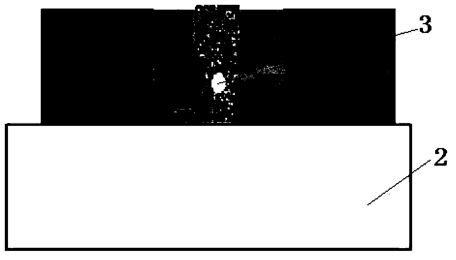
[0040] The chip made by adopting this embodiment can effectively avoid the generation of pores 3 during the filling process due to the improved gap filling ability of the spacer, and avoid subsequent filling materials from diffusing from the pores, thereby avoiding the occurrence of pr...


PUM


Abstract

The invention relates to a method for improving a gap filling capability. The method comprises the following steps: step one, carrying out etching to form a spacer region having a certain depth-to-width ratio; step two, carrying out secondary etching on the spacer region; and step three, carrying out corresponding filling on the spacer region according to the requirement of the method. According to the method, primary and secondary etching or acid pickling processes are added based on the traditional method; the depth-to-width ratio of the spacer region is reduced; and the gap filling capability during the chip manufacturing is enhanced. The possibility of hole occurrence during the filling process is reduced with the enhancement of the gap filling capability, so that the possibility of occurrence of problems of short circuit and the like due to the hole existence is also reduced; and hence, the electrical stability of the chip is enhanced, thereby improving the yield of the finished chip and the economic benefits.

Description

technical field [0001] The invention relates to the field of manufacturing semiconductor devices, in particular to a method for improving gap filling capability. Background technique [0002] In the semiconductor method, the component size of the integrated circuit is required to be smaller and smaller, so that more components can be accommodated on a semiconductor chip. As the circuit edge becomes smaller and faster, the distance between the components is also getting smaller and smaller. Based on the special requirements of electrical breakdown, a wider spacer is required as a barrier layer. However, due to the small line width characteristics of the semiconductor method, the width of the barrier layer will make the spacing between Poly narrower, and Its depth will not change because of these, which leads to a large depth-to-width ratio between Polys, resulting in a reduction in the subsequent filling capacity. In the subsequent filling, pores are easy to be generated, and...

Claims


Application Information

Patent Timeline
Patent Type & Authority Applications(China)
IPC IPC(8): H01L21/02H01L21/311
Inventor 张建伟洪文田赵丹朱东亮
Owner HEJIAN TECH SUZHOU
Why Eureka
Try Eureka