Transparent conducting oxide film-plated glass and preparation method thereof
A transparent conductive, coated glass technology, applied in chemical instruments and methods, glass/slag layered products, layered products, etc., can solve problems such as narrow sunlight spectrum
- Summary
- Abstract
- Description
- Claims
- Application Information
AI Technical Summary
Problems solved by technology
Method used
Image
Examples
preparation example Construction
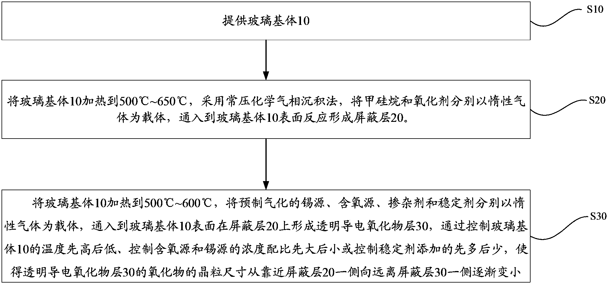
[0039] like figure 2 The preparation method of the transparent conductive oxide-coated glass of one embodiment shown includes the following steps:
[0040] S10 , providing a glass substrate 10 .
[0041] The glass substrate 10 can be 1mm-5mm thick soda-lime ordinary flat colorless glass or low-iron ultra-clear flat glass.
[0042] After the glass substrate 10 is cleaned and dried, it can be used to prepare transparent conductive oxide-coated glass.
[0043] S20 , heating the glass substrate 10 to 500° C. to 650° C., using an atmospheric pressure chemical vapor deposition method, passing monosilane and an oxidizing agent respectively into the surface of the glass substrate 10 with an inert gas as a carrier, and reacting to form a shielding layer 20 .
[0044] Atmospheric pressure chemical vapor deposition (APCVD) is used in the coating area of the furnace body, and monosilane and oxidant are respectively used as carriers of inert gas, and passed into S10 at 500°C~650°C to ...
Embodiment 1
[0065] In the APCVD reaction chamber, the glass substrate successively passes through the reaction zone with a space temperature of 620°C and 600°C, the concentration of monosilane is 0.1% and 0.15% by mole percentage, and the oxygen concentration ratio is 10% by mole percentage. % and 15%, the shielding layer made of silicon dioxide film material with a comprehensive refractive index of 1.52 and a thickness of 55nm was deposited.
[0066] The glass substrate that has been deposited with the shielding layer is introduced into the tin dioxide film deposition chamber, and the tin dioxide film is deposited three times successively. The reaction conditions are as follows:
[0067]
[0068] It is measured that the prepared transparent conductive oxide layer has a sheet resistance of 9Ω / □ and a transmittance of 80.2%. The single-point haze at 550nm is 16.2%, and the average haze at 380nm~780nm is 15.5%.
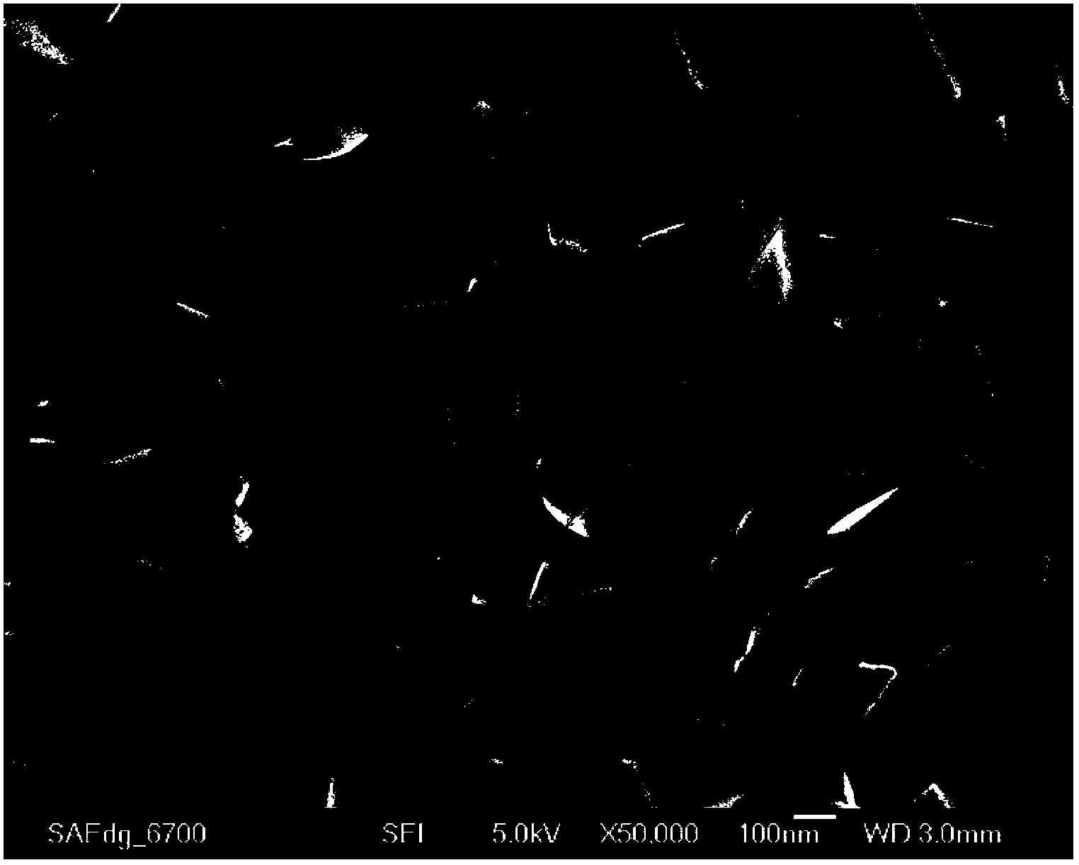
[0069] Depend on image 3 and Figure 4 It can be seen that the crystal ...
Embodiment 2
[0071] In the APCVD reaction chamber, the glass substrate successively passes through the reaction zone with a space temperature of 620°C and 620°C, the concentration of monosilane is 0.08% and 0.12% by mole percentage, and the oxygen concentration ratio is 15% by mole percentage. % and 20%, the shielding layer made of silicon dioxide with a comprehensive refractive index of 1.55 and a thickness of 60nm was deposited.
[0072] The glass substrate that has been deposited with the shielding layer is introduced into the tin dioxide film deposition chamber, and the tin dioxide film is deposited twice successively. The reaction conditions are as follows:
[0073]
[0074] It is measured that the prepared transparent conductive oxide layer has a sheet resistance of 8.9Ω / □ and a transmittance of 80.8%. The single-point haze at 550nm is 14.3%, and the average haze at 380nm~780nm is 12.9%.
PUM
| Property | Measurement | Unit |
|---|---|---|
| thickness | aaaaa | aaaaa |
| thickness | aaaaa | aaaaa |
| thickness | aaaaa | aaaaa |
Abstract
Description
Claims
Application Information


