Preparation method of high K hafnium dioxide amorphous film

A hafnium dioxide and amorphous thin film technology, which is applied in ion implantation plating, metal material coating process, coating, etc., can solve the problem of incomplete formation of amorphous thin film, and achieve the suppression of multiphase mixing and optimization of structure Proportion, good compactness effect

Inactive Publication Date: 2013-12-18
UNIV OF ELECTRONIC SCI & TECH OF CHINA
View PDF3 Cites 7 Cited by
  • Summary
  • Abstract
  • Description
  • Claims
  • Application Information

AI Technical Summary

Problems solved by technology

[0003] The purpose of the invention is to overcome the current HfO 2 The preparation process of thin film materials is made by doping or heating, and the disadvantage of not being able to completely form amorphous thin films is to provide a preparation method for high-K hafnium dioxide amorphous thin films

Method used


Image

  • Preparation method of high K hafnium dioxide amorphous film
  • Preparation method of high K hafnium dioxide amorphous film

Examples


Embodiment

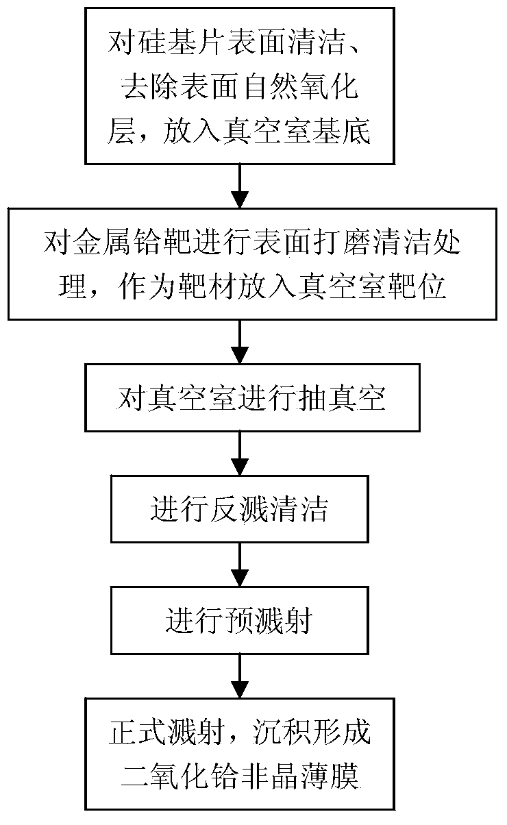
[0026] In this example, QX-500 high-vacuum multifunctional coating equipment is used. The preparation method of the high-K hafnium dioxide amorphous film in this example includes the following steps:

[0027] A. Clean the surface of the silicon substrate, remove the natural oxide layer on the surface of the silicon substrate, and put it into the base of the vacuum chamber.

[0028] In this step, the silicon substrate is a single-polish silicon substrate with n-type crystal orientation (100) of 10mm×10mm. This step is specifically: clean the silicon substrate with an ultrasonic cleaner in acetone and alcohol for a fixed period Carry out surface cleaning treatment, the fixed time is 10 to 15 minutes, after drying, soak in a certain concentration of hydrofluoric acid solution for a period of time to remove the natural oxide layer on the surface of the silicon substrate, the certain concentration can be about 5% , the period of time is 1 to 2 minutes, the silicon substrate is clea...


PUM


Abstract

The invention relates to a semiconductor technology, and provides a preparation method of a high K hafnium dioxide amorphous film, which solves the problem that preparation processes of existing HfO2 film materials adopt a doping or heating mode to prepare the HfO2 film materials so that amorphous films can not be entirely generated. The preparation method comprises the following steps: firstly putting a silicon substrate into a vacuum chamber base after the surface of the silicon substrate is cleaned and a natural oxidation layer on the surface is removed, secondly putting a metal hafnium target with surface polished and cleaned into a target position in a vacuum chamber as a target, closing a target baffle, utilizing high vacuum multifunctional radio frequency sputtering coating equipment to vacuumize the vacuum chamber, carrying out backwash cleaning on the substrate, switching on a radio frequency power supply and adjusting the power of the radio frequency power supply after backwash cleaning, carrying out pre-sputtering, finally adjusting the argon flux, filling oxygen and opening the target baffle to formally sputter a hafnium dioxide film, thus forming the hafnium dioxide amorphous film. The preparation method has the beneficial effects that crystallization of the hafnium dioxide film can not be caused, and the preparation method is suitable for preparation of the hafnium dioxide amorphous film.

Description

technical field [0001] The present invention relates to semiconductor technology, in particular to high dielectric constant HfO 2 (HfO2) amorphous film. Background technique [0002] The development of semiconductor integrated circuits puts forward higher requirements for the density and performance of integrated circuits. The thickness of the gate dielectric film of typical CMOS devices becomes thinner and thinner, and begins to approach the atomic distance gradually. Due to the direct tunneling of the gate dielectric oxide layer The leakage current and static power loss caused by wear and tear will increase significantly. Therefore, conventional silicon dioxide (SiO 2 ) The gate dielectric is increasingly approaching its limit. Replacement of SiO with high dielectric constant (high K) thin film materials 2 It is currently the most promising way to solve this problem. Using this material can allow the thickness of the insulating layer to be increased without increasing...

Claims


Application Information

Patent Timeline
IPC IPC(8): C23C14/40C23C14/54C23C14/08
Inventor 唐武杨宇桐
Owner UNIV OF ELECTRONIC SCI & TECH OF CHINA
Why Eureka
Try Eureka