Manufacturing method of germanium-silicon heterojunction bipolar triode device

A technology of heterojunction bipolar, manufacturing method, applied in semiconductor/solid-state device manufacturing, electrical components, circuits, etc., can solve problems such as process instability, increased defects, base-collector junction leakage, etc., and achieve stability Process flow, process cost reduction, and the effect of high product yield

Active Publication Date: 2013-12-18
SHANGHAI HUAHONG GRACE SEMICON MFG CORP
View PDF4 Cites 3 Cited by
  • Summary
  • Abstract
  • Description
  • Claims
  • Application Information

AI Technical Summary

Problems solved by technology

[0003] The silicon-germanium heterojunction in the silicon-germanium heterojunction bipolar transistor is the core of the device. In the conventional process, a layer of amorphous silicon is introduced, so in order to reduce the formation of silicon-germanium in the subsequent growth of the silicon-germanium epitaxial layer Defects need to be pre-treated at a high temperature higher than 900 degrees, and the amorphous silicon recrystallizes at high temperatures, making the surface of the device very rough, which will cause subsequent processes to be affected by this, such as photolithography can not be aligned, defects increase, substrate Electrode-collector junction leakage, process instability and other issues seriously affect the yield of products

Method used


Image

  • Manufacturing method of germanium-silicon heterojunction bipolar triode device
  • Manufacturing method of germanium-silicon heterojunction bipolar triode device
  • Manufacturing method of germanium-silicon heterojunction bipolar triode device

Examples


Embodiment Construction

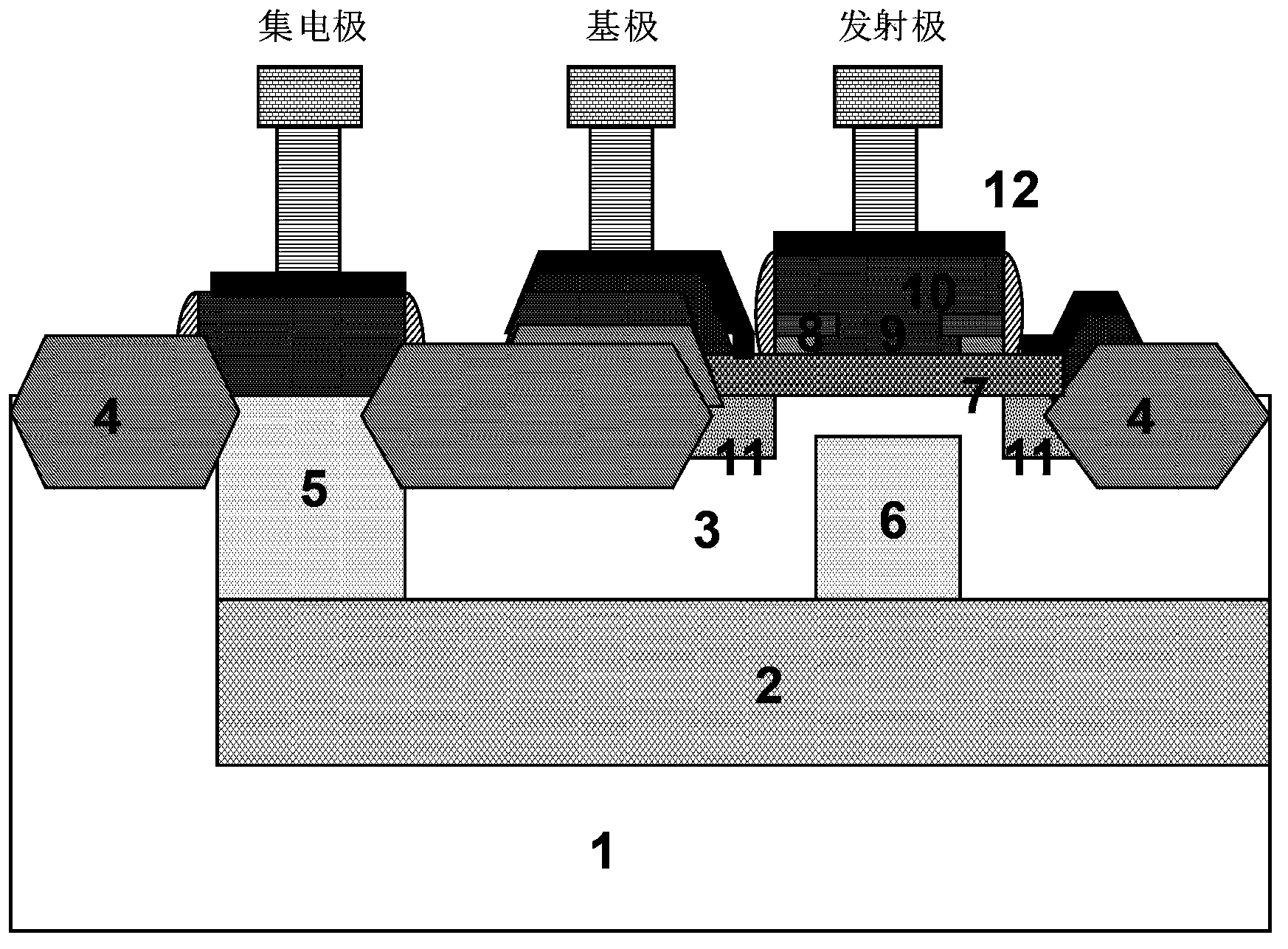
[0026] The present invention will be further described in detail below in conjunction with the accompanying drawings and specific embodiments.

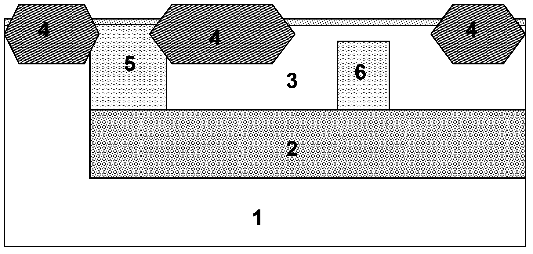
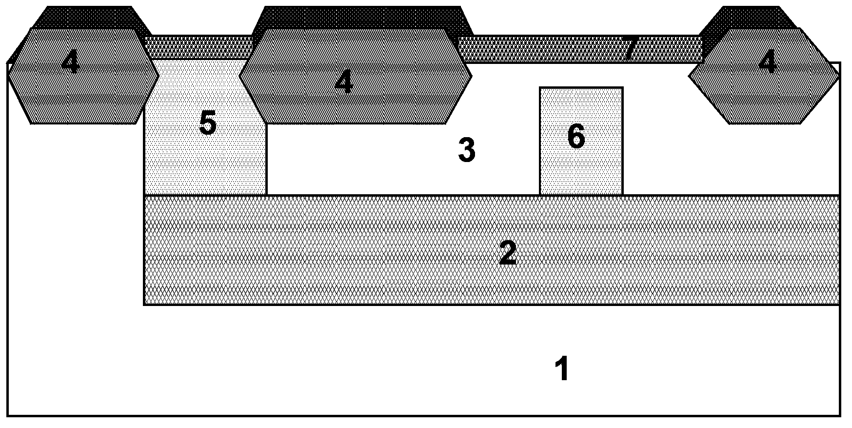
[0027] The manufacturing method of silicon germanium heterojunction bipolar transistor device of the present invention, as Figure 11 shown, including the following steps:

[0028] Step 1, forming an N-type buried layer 2 on the P-type silicon substrate 1, the N-type buried layer 2 is heavily doped, the implanted ions are impurity arsenic that diffuses less upwardly when the thermal overhead is high, and the implantation energy is 30 ~120keV, the dose is 10 15 ~10 16 cm -2 Carry out high-temperature propulsion using a furnace tube, the propulsion temperature is 1000-1100°C, and the time is 30-120 minutes, and then low N-doped epitaxy 3 growth is performed on the N-type buried layer 2, and the doped impurity is phosphorus. The impurity concentration is 2×10 15 ~5×10 16 cm -3 ; Perform N-type ion implantation on the N-type buried...


PUM


Abstract

The invention discloses a manufacturing method of a germanium-silicon heterojunction bipolar triode device. The method includes that a current collecting area is prepared by a low-doping N-type epitaxial process, a heavy N-type doped low-resistance buried layer passage is arranged at the bottom, and high-dose middle-energy N-type ions are injected in a current collecting electrode active area to form a current collecting electrode leading-out end; after an isolation area is formed, surface cleaning and growing of a germanium-silicon epitaxial layer of a thick buffering layer are performed, the germanium-silicon epitaxial layer outside a base area and an outer base area is defined by photoetching and removed by dry-etching; an emitting electrode window medium is deposited, an emitting electrode window and the whole current collecting electrode active area are opened by photoetching, dry-etching and wet-etching, N-type heavily-doped emitting electrode polysilicon is deposited, and an N-type emitting electrode-base electrode junction and a lower-resistance passage are formed. Polysilicon thickness of the outer base area is increased by adjusting thickness of the germanium-silicon buffering layer, so that resistance performance of the base area is guaranteed, process cost is lowered, and more stable technological process and higher product yield are acquired.

Description

technical field [0001] The invention relates to the field of semiconductor integrated circuits, in particular to a method for manufacturing a germanium-silicon heterojunction bipolar triode power device. Background technique [0002] In the conventional germanium-silicon heterojunction bipolar transistor process, after the collector region is formed, a thin layer of silicon oxide is grown by thermal oxidation to remove silicon surface damage; a layer of silicon oxide and a layer of amorphous silicon are deposited , the base active area is opened by photolithography and dry etching of amorphous silicon, while the collector active area and other active areas are protected by the above-mentioned silicon oxide and amorphous silicon; wet removal of exposed silicon oxide and cleaning Silicon germanium epitaxial growth is carried out on the silicon surface, and the silicon germanium epitaxial layer grown on the exposed base area active region has a single crystal silicon structure,...

Claims


Application Information

Patent Timeline
Patent Type & Authority Applications(China)
IPC IPC(8): H01L21/331
Inventor 周正良周克然陈曦
Owner SHANGHAI HUAHONG GRACE SEMICON MFG CORP
Why Eureka
Try Eureka