

Manufacturing method of nanometer laser device laser-bundling device
A nano-laser and laser beam-combining technology, applied in nano-optics, nano-technology, nano-technology and other directions, can solve the problem of limited laser power and achieve the effect of compact structure, stable performance and easy processing
- Summary
- Abstract
- Description
- Claims
- Application Information
AI Technical Summary
Problems solved by technology
Method used
Image

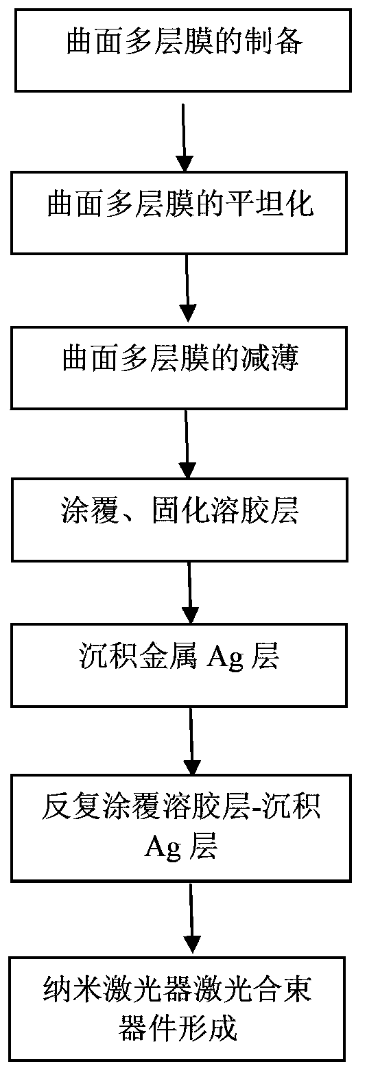
Examples
Embodiment 1
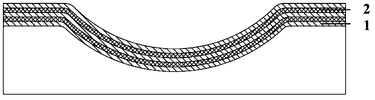
[0031] Example 1, such as figure 1 As shown, a nanolaser laser beam combining device is prepared on a curved surface groove with a diameter depth of 200nm, and the specific implementation steps are as follows:
[0032] (1) Deposit a curved multilayer film structure on a curved groove. Metal Ag and dielectric SiO are alternately deposited by magnetron sputtering deposition 2 , in which the metal Ag is deposited by DC sputtering with a DC power of 120w; the dielectric SiO 2 Radio frequency sputtering is used for deposition, and the deposition power is 200w. The film thickness of each layer is 20nm. A total of 10 groups of 20 layers were deposited, with a total film thickness of 400nm, such as figure 2 Shown; 1 represents metal Ag; 2 represents silicon dioxide.
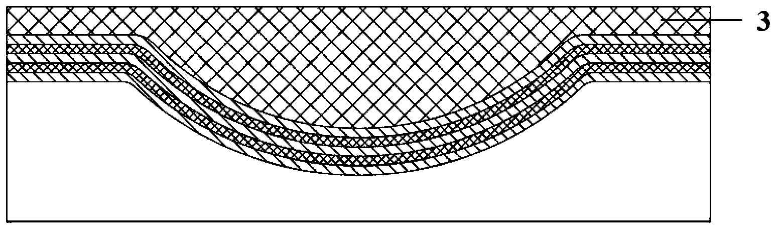
[0033] (2) Planarization is carried out by coating AZ-3100 photoresist, the rotation speed is 4000rpm, the spin coating time is 40s, and baked on a hot plate at 120°C for 1h. The glue thickness is 1000nm, such as ...
Embodiment 2
[0038] Embodiment 2, in such as figure 1 As shown, a nanolaser laser beam combining device is prepared on a curved surface groove with a diameter depth of 250 nm, and the specific implementation steps are as follows:
[0039] (1) Deposit a curved multilayer film structure on the prepared curved groove. Deposition by evaporation coating, alternate deposition of metal Ag and dielectric SiO 2 , where the metal Ag is deposited by thermal evaporation, and the dielectric SiO 2 Deposited by electron beam evaporation. The film thickness of each layer is 30nm. A total of 8 groups of 16 layers were deposited, with a total film thickness of 480nm, such as figure 2 Shown; 1 represents metal Ag; 2 represents silicon dioxide.
[0040] (2) Planarization is carried out by coating AR-P3120 photoresist sol layer, the rotation speed is 5000rpm, the suspension coating time is 40s, and baked on a hot plate at 100°C for 1h. The glue thickness is 600nm, such as image 3 Shown; 3 represents t...
Embodiment 3
[0045] Example 3, such as figure 1 As shown, a nanolaser laser beam combining device is prepared on a curved surface groove with a diameter depth of 300nm, and the specific implementation steps are as follows:
[0046] (1) Deposit a curved multilayer film structure on a curved groove. Magnetron sputtering was used to deposit metal Ag and medium SiO2 alternately, wherein metal Ag was deposited by DC sputtering with a DC power of 120w; medium SiO2 was deposited by radio frequency sputtering with a deposition power of 200w. The film thickness of each layer is 15nm. A total of 20 groups of 40 layers were deposited, with a total film thickness of 600nm, such as figure 2 Shown; 1 represents metal Ag; 2 represents silicon dioxide.
[0047] (2) Planarization is carried out by coating AR-P3170 photoresist, the rotation speed is 2000rpm, the spin coating time is 40s, and the coating is repeated 5 times. Bake on a hot plate at 120 °C for 1 h. The glue thickness is 600nm, such as ...
PUM
| Property | Measurement | Unit |
|---|---|---|
| Thickness | aaaaa | aaaaa |
| Thickness | aaaaa | aaaaa |
Abstract
Description
Claims
Application Information