Method for directly synthesizing high conductivity nickel sulfide two-dimension nanosheet array in large scale
A two-dimensional nanotechnology with high conductivity, applied in nickel sulfide, nanotechnology, nanotechnology, etc., can solve the problems of complex process steps and lower production efficiency, and achieve easy control of preparation parameters, good repeatability, and simple process Effect
- Summary
- Abstract
- Description
- Claims
- Application Information
AI Technical Summary
Problems solved by technology
Method used
Image
Examples
Embodiment 1
[0025] Weigh 0.05g of nickel ethylxanthate powder and put it in a vacuum drying oven, place the glass sheet near the nickel ethylxanthate powder, heat to 160°C, keep it warm for 300 minutes, cool to room temperature, take out the glass sheet, and you can find A uniform film was formed on the glass slide.
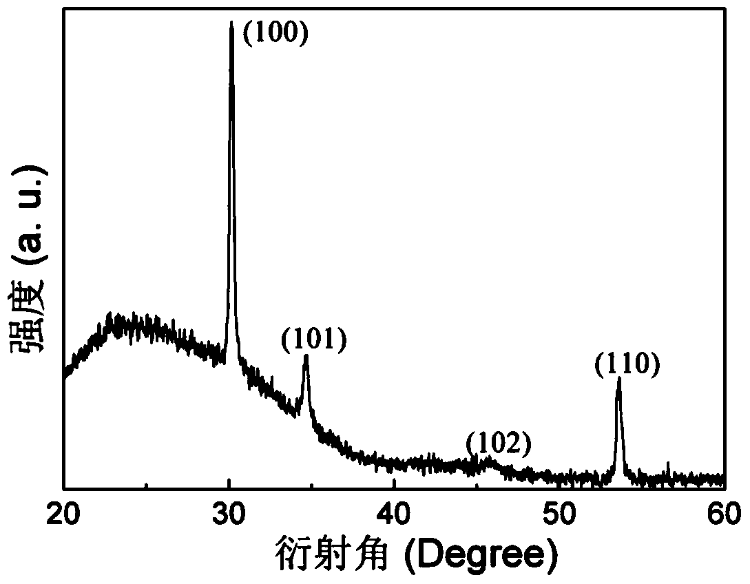
[0026] figure 1 It is the X-ray diffraction pattern of nickel sulfide nanosheet array, which can confirm that this is nickel sulfide with hexagonal structure.
[0027] figure 2 is a scanning electron micrograph of nickel sulfide nanosheet arrays. It can be seen from the figure that the array of nickel sulfide nanosheets is evenly distributed on the glass surface, and the thickness of the nanosheets is about 10 nanometers.
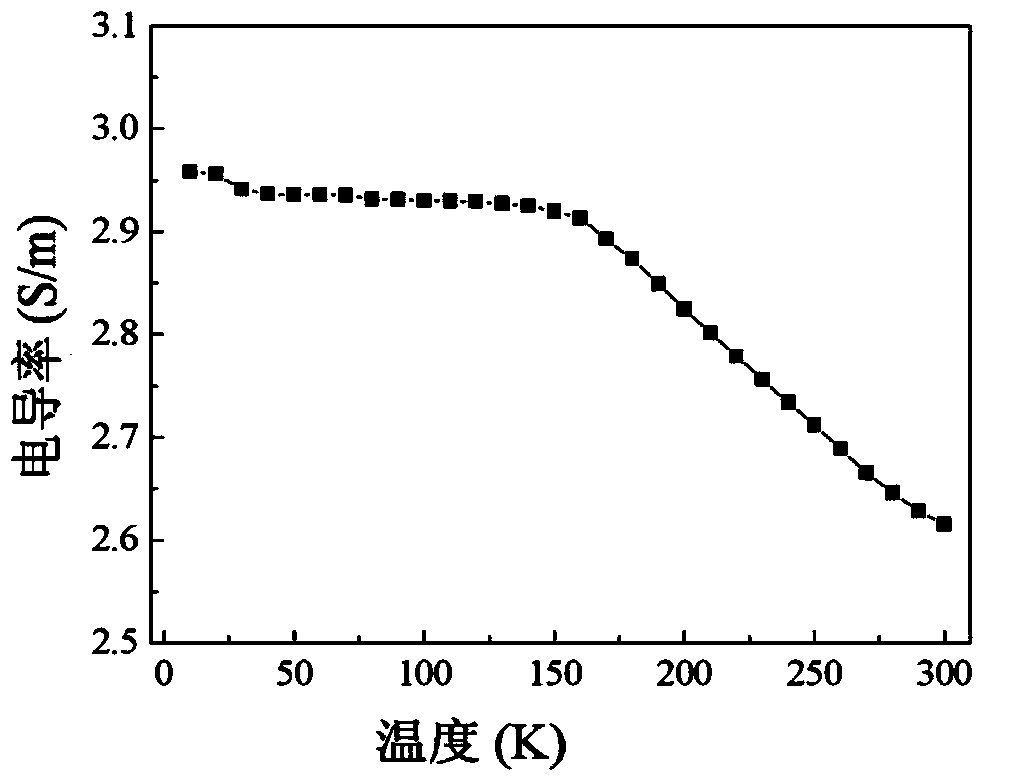
[0028] image 3 is the conductivity curve of the nickel sulfide nanosheet array. It can be seen from the figure that the room temperature conductivity of nickel sulfide nanosheet array is as high as 2.6×10 5 S / m.
Embodiment 2
[0030] Weigh 0.3g of nickel isobutyl xanthate powder into a box-type resistance furnace, place a polyimide plastic sheet near the nickel isobutyl xanthate powder, heat to 220°C, keep it warm for 80 minutes, and cool to room temperature Take out the polyimide plastic sheet, and it can be found that a uniform film is formed on the polyimide plastic sheet.
[0031] Figure 4 A scanning electron micrograph of nickel sulfide nanosheet arrays. It can be seen from the figure that the nickel sulfide nanosheet array is evenly distributed on the surface of the polyimide plastic sheet, and the thickness is about 15-20 nanometers.
Embodiment 3
[0033] Weigh 0.1g of nickel propylxanthate powder and put it into a tube-type resistance furnace, place the silicon chip near the nickel propylxanthate powder, heat to 360°C, keep it warm for 10 minutes, cool to room temperature and take out the silicon chip. It was found that a uniform thin film was formed on the silicon wafer.
PUM
| Property | Measurement | Unit |
|---|---|---|
| thickness | aaaaa | aaaaa |
| thickness | aaaaa | aaaaa |
Abstract
Description
Claims
Application Information


