

Preparation method of polycrystalline silicon
A technology of polysilicon and broken polysilicon, which is applied in the field of solar cells, can solve the problems of increased hard point content in silicon ingots, low battery conversion efficiency, and complicated process operations, so as to achieve uniform crystal grains and reduce the risk of sticking pots. The effect of low dislocation defects
- Summary
- Abstract
- Description
- Claims
- Application Information
AI Technical Summary
Problems solved by technology
Method used
Image


Examples
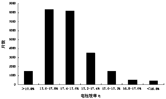
Embodiment 1
[0047] (1) Quartz crucible pretreatment: 24 hours before feeding, mix 400g of high-purity silicon powder with 500mL of absolute ethanol, stir to form a slurry, brush evenly on the bottom of the crucible with a brush, and thicken the bottom of the crucible, and dry it for later use ;
[0048] (2) Spread 20kg of scrap material on the bottom of the pretreated quartz crucible, put silicon material (810kg in total) and 108g of silicon-boron alloy into the quartz crucible, feed the material, vacuumize in the 850-type G6 polysilicon ingot furnace, and heat The silicon material is melted; the doping amount of the master alloy is calculated according to the GB-T 13389-1992 standard for conversion of boron-doped phosphorus-doped silicon single crystal resistivity and dopant concentration.
[0049](3) At the end of the melting step, the temperature of the heater is controlled at 1560°C, the heat insulation cage is raised to the opening a of 10mm, and the temperature of TC2 is controlled ...
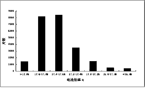
Embodiment 2
[0058] (1) Quartz crucible pretreatment: 24 hours before feeding, mix 400g of high-purity silicon powder with 450mL of absolute ethanol, stir to form a slurry, brush evenly on the bottom of the crucible with a brush, and thicken the bottom of the crucible, and dry it for later use ;
[0059] (2) Spread 20kg of scrap material on the bottom of the pretreated quartz crucible, put silicon material (810kg in total) and 100g of silicon-boron alloy into the quartz crucible, feed the material, vacuumize in the 850-type G6 polysilicon ingot furnace, and heat The silicon material is melted; the doping amount of the master alloy is calculated according to the GB-T 13389-1992 standard for conversion of boron-doped phosphorus-doped silicon single crystal resistivity and dopant concentration.
[0060] (3) At the melting end step, the temperature of the heater is controlled at 1565°C, the heat insulation cage is raised to the opening a of 10mm, and the temperature of TC2 is controlled not to...
PUM
| Property | Measurement | Unit |
|---|---|---|
| particle diameter | aaaaa | aaaaa |
| thickness | aaaaa | aaaaa |
Abstract
Description
Claims
Application Information