

Preparation method of gallium oxide-doped membrane and gallium oxide-doped membrane
A gallium oxide film and gallium oxide technology, which is applied in the field of semiconductor material preparation, can solve problems such as the difficulty in realizing multiple types of gallium oxide films, safety, and effective doping, and achieve the effect of scientific steps and excellent conductive properties
- Summary
- Abstract
- Description
- Claims
- Application Information
AI Technical Summary
Problems solved by technology
Method used
Image

Examples
preparation example Construction
[0027] The invention discloses a method for preparing a doped gallium oxide film suitable for a metal organic chemical vapor deposition system. The method specifically includes the following steps:
[0028] In order to achieve the above object, the technical solution adopted in the present invention is: a method for preparing a doped gallium oxide film, comprising the following steps:
[0029] 1) Select the substrate, which contains the target doping element, that is, the substrate is the doping source;
[0030] 2) Preparing a gallium oxide film on the substrate by metal-organic chemical vapor deposition to obtain a primary doped gallium oxide film;
[0031] 3) Heat treatment and activation of the prepared doped gallium oxide film to obtain a doped gallium oxide film containing target doping elements.
[0032] The substrate mentioned in this method is a single substrate or a composite substrate with a pre-deposited layer. When the substrate is a single substrate, the gallium...
Embodiment 1
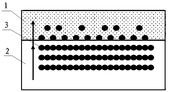
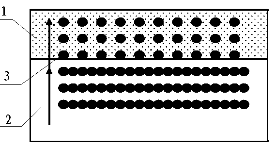
[0043] figure 1 It is a schematic diagram of the diffusion of arsenic atoms from the gallium arsenide substrate to the gallium oxide film in embodiment 1; figure 2It is a schematic diagram of the continuous diffusion of arsenic atoms from the substrate to the gallium oxide film during the annealing treatment in Example 1.
[0044] The invention relates to a method for preparing an arsenic-doped gallium oxide film, which uses a single substrate (single crystal gallium arsenide), such as figure 1 and figure 2 As shown, specifically the preparation method of the arsenic-doped gallium oxide film comprises the following steps:
[0045] Step 1: Select single crystal gallium arsenide 2 as the epitaxial substrate, and at the same time as the doping source of arsenic 3 . The substrate is cleaned for use.
[0046] Step 2: Use metal-organic chemical vapor deposition equipment to grow gallium oxide film 1 on a single crystal gallium arsenide 2 substrate, set the growth temperature o...
Embodiment 2
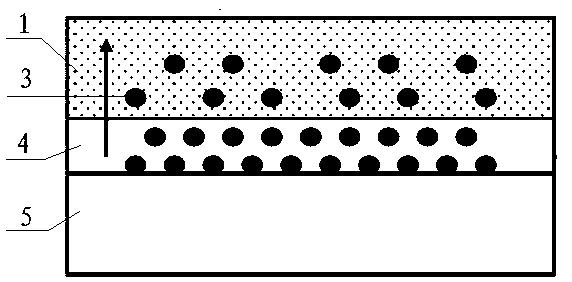
[0053] image 3 It is a schematic diagram of the diffusion of arsenic atoms from the pre-deposited arsenic single substance layer on the sapphire substrate to the gallium oxide film in embodiment 2; Figure 4 It is a schematic diagram of the redistribution of arsenic atoms in the gallium oxide film during the subsequent annealing treatment in Example 2.
[0054] The invention relates to a method for preparing an arsenic-doped gallium oxide film, which uses a composite substrate (the pre-deposited layer is a simple layer of arsenic), such as image 3 and Figure 4 As shown, specifically the preparation method of the arsenic-doped gallium oxide film comprises the following steps:
[0055] Step 1: Select the sapphire 5 with the arsenic elemental layer 4 pre-deposited on its surface as the composite substrate, and the arsenic 3 in the pre-deposited arsenic elemental layer as the dopant source.
[0056] Step 2: Use metal-organic chemical vapor deposition equipment to grow galliu...
PUM
 Abstract
Description
Claims
Application Information