Doping method for p-type zinc telluride single crystal thin-film material

A single crystal thin film, zinc telluride technology, applied in the direction of electrical components, semiconductor/solid-state device manufacturing, circuits, etc., can solve problems such as unevenness, complicated process control, and difficult precise control of doping concentration, so as to inhibit the volatilization of tellurium element , less damage, easy to implement effect

Inactive Publication Date: 2013-12-25
INST OF SEMICONDUCTORS - CHINESE ACAD OF SCI
View PDF5 Cites 5 Cited by
  • Summary
  • Abstract
  • Description
  • Claims
  • Application Information

AI Technical Summary

Problems solved by technology

The in-situ doping method is easy to prepare high-quality zinc telluride single crystal thin films with uniform doping concentration, but there is a problem of complicated process control; the ion implantation method has the advantages of precise controllable doping concentration, simple process, and can achieve selective doping However, a certain degree of lattice defects will be generated in the thin film crystal, especially in the surface layer, and rapid thermal annealing must be done to repair the crystal defects and activate the electrical activity of doping elements; the process of thermal diffusion method is very simple, but The doping concentration is not easy to control accurately, and it is also very uneven. The high temperature process takes a long time and is easy to damage the steep interface of the heterogeneous structure of the device material. It is only used in individual cases.

Method used


Image

  • Doping method for p-type zinc telluride single crystal thin-film material
  • Doping method for p-type zinc telluride single crystal thin-film material
  • Doping method for p-type zinc telluride single crystal thin-film material

Examples


Embodiment Construction

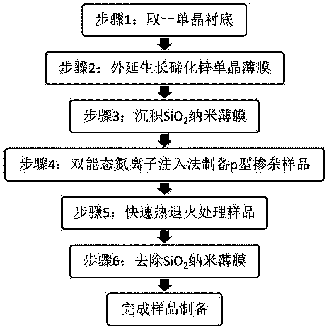
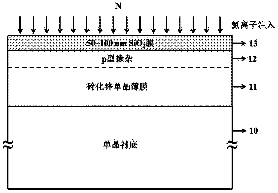
[0016] see figure 1 with figure 2 As shown, the present invention provides a method for doping a p-type zinc telluride single crystal thin film material, comprising the steps of:

[0017] Step 1: Take a single crystal substrate 10, and the material of the single crystal substrate 10 is ZnTe, GaSb, GaAs or Si wafer. For example: choose the ready-to-use 2-inch semi-insulating GaAs (001) wafer as the substrate material.

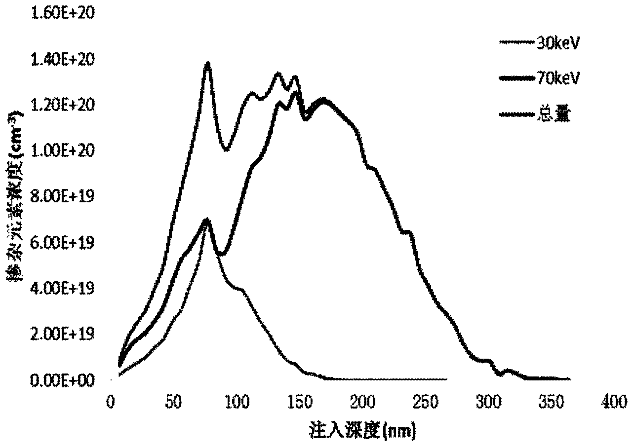
[0018] Step 2: On the single crystal substrate 10, epitaxially grow a single crystal thin film 11, the single crystal thin film 11 is not intentionally doped, and its thickness is greater than 100nm, and the epitaxial growth single crystal thin film 11 adopts molecular beam epitaxy or metal organic chemical vapor deposition. For example: use molecular beam epitaxy growth equipment to grow zinc telluride single crystal thin film materials heterogeneously. In the experiment, Zn and Te with a purity of 6N (≥99.9999%) were selected as the molecular beam source,...


PUM

PropertyMeasurementUnit
thicknessaaaaaaaaaa
thicknessaaaaaaaaaa

Abstract

Provided is a doping method for a p-type zinc telluride single crystal thin-film material. The method comprises the following steps that 1, a single crystal substrate is extracted; 2, a single crystal thin film is grown on the single crystal substrate in an epitaxial mode; 3, a layer of a SiO2 nano film is deposited on the surface of the single crystal thin film; 4, a double-energy-state nitrogen ion injection method is utilized, nitrogen is injected downwards from the surface of the SiO2 nano film, a p-type doping layer is formed on the lower face of the SiO2 nano film, and a sample is formed; 5, rapid thermal annealing processing is carried out on the sample; 6, the SiO2 nano film on the surface of the sample is removed, and preparation is achieved. The doping method is compatible with an existing microelectronic device manufacturing process and is easy to implement. In addition, the method can also be suitable for p-type doping of an intrinsic zinc telluride single crystal surface, and can provide a reference for p-type doping experiments for semiconductor thin-film materials of chemical compounds of other II-VI groups.

Description

technical field [0001] The invention belongs to the technical field of semiconductor material preparation, and relates to a doping method of a p-type zinc telluride single crystal thin film material, in particular to a p-type doped zinc telluride single crystal thin film material prepared by using a dual-energy state nitrogen ion implantation method Methods. Background technique [0002] Zinc telluride is an important II-VI compound semiconductor material with a bandgap width of 2.26eV at room temperature, which belongs to the direct bandgap energy band structure. Zinc telluride has good application prospects in the manufacture of green light-emitting diodes (LEDs), solar cells, terahertz detectors, optical waveguides and other optoelectronic devices. Due to the difficulty in growing zinc telluride bulk single crystal materials, small wafer size and high price, most of the common zinc telluride devices are fabricated on heteroepitaxially grown thin films. At present, the c...

Claims


Application Information

Patent Timeline
Patent Type & Authority Applications(China)
IPC IPC(8): H01L21/265
Inventor 刘超张理嫩杨秋旻崔利杰曾一平
Owner INST OF SEMICONDUCTORS - CHINESE ACAD OF SCI
Why Eureka
Try Eureka