
Gold and silver alloy bonding wire with gold-plated layer on surface and preparation method thereof

A technology of gold-silver alloy and gold-plated layer, applied in the field of gold-silver alloy bonding wire and its preparation, can solve problems such as incompatibility, and achieve the effects of smooth surface, low price, and reduced packaging cost

Active Publication Date: 2013-12-25
辽宁凯立尔电子科技有限公司
View PDF7 Cites 18 Cited by
  • Summary
  • Abstract
  • Description
  • Claims
  • Application Information

AI Technical Summary

Problems solved by technology

Therefore, silver alloy gold-plated bonding wire is not suitable for packaging of LED, COB and multi-pin integrated circuits

Method used


Image

  • Gold and silver alloy bonding wire with gold-plated layer on surface and preparation method thereof
  • Gold and silver alloy bonding wire with gold-plated layer on surface and preparation method thereof
  • Gold and silver alloy bonding wire with gold-plated layer on surface and preparation method thereof

Examples


Embodiment 1

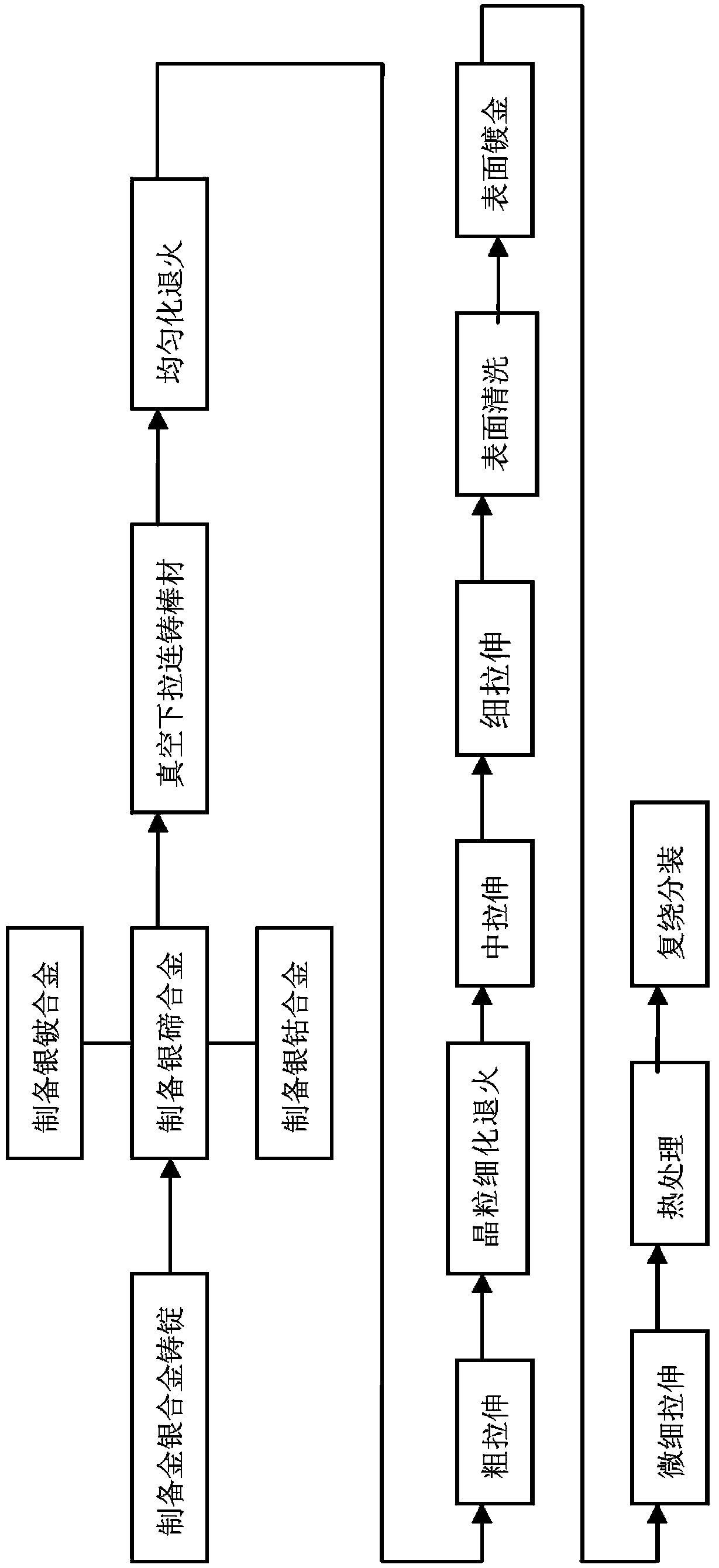
[0070] 1) Select silver ingots with a purity of ≥99.99% and gold ingots with a purity of ≥99.99%, first wash them with 10% sodium hydroxide, then rinse them with deionized water, and dry them in an oven for later use.

[0071] 2) Preparation of gold and silver alloy ingots: put silver ingots with a purity of ≥99.99% and gold ingots with a purity of ≥99.99% in proportion to a high-purity graphite crucible, place them in a vacuum melting furnace, and conduct intermediate frequency induction heating to 1100 ℃, during the heating process, vacuum treatment; after the material is completely melted, fill it with high-purity nitrogen and keep it warm for 30 minutes; pour the liquid gold-silver alloy into a high-purity graphite tank to obtain gold and silver with a width of 5 cm, a thickness of 1 cm, and a gold content of 7%. Alloy ingots.

[0072] 3) Preparation of silver-beryllium alloy rods: put 99.99% pure silver and trace element beryllium in a high-purity graphite crucible,...

Embodiment 2

[0087] 1) Select silver ingots with a purity of ≥99.99% and gold ingots with a purity of ≥99.99%, first wash them with 17.5% sodium hydroxide, then rinse them with deionized water, and dry them in an oven for later use.

[0088] 2) Preparation of gold and silver alloy ingots: put silver ingots with a purity of ≥99.99% and gold ingots with a purity of ≥99.99% in proportion to a high-purity graphite crucible, place them in a vacuum melting furnace, and conduct intermediate frequency induction heating to 1200 ℃, during the heating process, vacuum treatment; after the material is completely melted, fill it with high-purity nitrogen and keep it warm for 60 minutes; pour the liquid gold-silver alloy into a high-purity graphite tank to obtain a gold with a width of 7.5cm, a thickness of 1cm, and a gold content of 7%. Silver alloy ingots.

[0089] 3) Preparation of silver-beryllium alloy rods: put 99.99% pure silver and trace element beryllium in a high-purity graphite crucible,...

Embodiment 3

[0104] 1) Select silver ingots with a purity of ≥99.99% and gold ingots with a purity of ≥99.99%, first wash them with 17.5% sodium hydroxide, then rinse them with deionized water, and dry them in an oven for later use.

[0105] 2) Preparation of gold and silver alloy ingots: put silver ingots with a purity of ≥99.99% and gold ingots with a purity of ≥99.99% in proportion to a high-purity graphite crucible, place them in a vacuum melting furnace, and conduct intermediate frequency induction heating to 1200 ℃, during the heating process, vacuum treatment; after the material is completely melted, fill it with high-purity nitrogen and keep it warm for 60 minutes; pour the liquid gold-silver alloy into a high-purity graphite tank to obtain a gold with a width of 7.5cm, a thickness of 1cm, and a gold content of 10%. Silver alloy alloy ingot.

[0106] 3) Preparation of silver-beryllium alloy rods: put 99.99% pure silver and trace element beryllium in a high-purity graphite cru...


PUM

PropertyMeasurementUnit
Widthaaaaaaaaaa
Thicknessaaaaaaaaaa
Diameteraaaaaaaaaa

Abstract

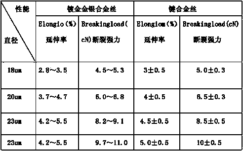
The invention belongs to the technical field of metal bonding wires used for microelectronic packaging, and particularly relates to a gold and silver alloy bonding wire with a gold-plated layer on the surface and a preparation method of the gold and silver alloy bonding wire. The gold and silver alloy bonding wire is good in push-pull effort, oxidation resistance and bonding performance and low in cost, and the gold-plated layer is arranged on the surface of the gold and silver alloy bonding wire. The gold and silver alloy bonding wire with the gold-plated layer on the surface comprises a gold and silver alloy wire and is structurally characterized in that a gold protective layer is arranged on the surface of the gold and silver alloy wire.

Description

technical field [0001] The invention belongs to the technical field of metal bonding wires for microelectronic packaging, and in particular relates to a gold-silver alloy bonding wire with a gold-plated layer on the surface and a preparation method thereof. Background technique [0002] Microelectronic wire bonding is a kind of microelectronic wire bonding that can be tightly welded to the substrate pad by using heat, pressure, and ultrasonic energy to realize the electrical interconnection between the chip and the substrate and the information exchange between the chips. Under ideally controlled conditions, electron sharing or interdiffusion of atoms occurs between the lead and the substrate, enabling atomic-scale bonding between the two metals. [0003] At present, in LDE, COB and multi-pin integrated circuit packages, gold wires and pure silver alloy gold-plated wires are mostly used for bonding wires. Due to the high price of the bonding gold wire, the packaging cost in...

Claims


Application Information

Patent Timeline
IPC IPC(8): H01L23/49H01L21/48C22C5/06C22F1/14
CPCH01L2224/45139H01L2224/45565H01L2224/45644H01L2924/00014H01L2224/45015H01L2224/45144H01L24/43H01L2224/43H01L2224/43848H01L2924/00011H01L2224/45H01L2224/48H01L2924/01079H01L2924/01004H01L2924/01052H01L2924/01027H01L2924/20751H01L2924/20752H01L2924/20753H01L2924/20754H01L2924/20755H01L2924/013H01L2924/00H01L2924/20108H01L2924/20109H01L2924/2011H01L2924/20111H01L2924/01049H01L2924/00012H01L2924/01005H01L2924/01204
Inventor 吴国防王东明吴瑞雪乌素华时阳张雷
Owner 辽宁凯立尔电子科技有限公司
Learn More