Back reflection electrode with periodic structure and manufacturing method thereof

A periodic structure and back reflection technology, applied in circuits, photovoltaic power generation, electrical components, etc., can solve the problems of low utilization rate of long-wavelength light, poor control of periodicity, and anodic oxidation caused by heat. Achieve good scattering, high scattering, and improved short-circuit current density

Active Publication Date: 2013-12-25
NANKAI UNIV
View PDF4 Cites 17 Cited by
  • Summary
  • Abstract
  • Description
  • Claims
  • Application Information

AI Technical Summary

Problems solved by technology

At present, the preparation method of the back reflector electrode with periodic structure is mainly anodized aluminum oxide (AAO). Due to the large amount of heat generated and the instability of anodic oxidation during the anodic oxidation process when the voltage is greater than 500V, its periodicity is not very good. control, and it is difficult to make a large size 'dimple' shape
Although the back reflective electrode prepared by the AAO method increases the scattering of short-wavelength light, the short-wave response of the battery is improved, and it has a light-trapping effect on short-wavelength light, but the light-trapping effect of long-wavelength light is due to its 'dimple' shape. Limited, resulting in low utilization of long-wavelength light by the battery

Method used


Image

  • Back reflection electrode with periodic structure and manufacturing method thereof
  • Back reflection electrode with periodic structure and manufacturing method thereof
  • Back reflection electrode with periodic structure and manufacturing method thereof

Examples


Embodiment 1

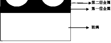
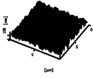
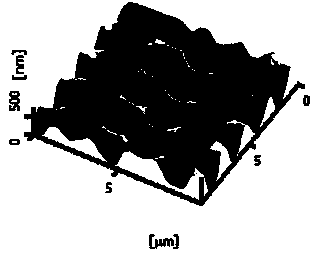
[0023] A periodically structured back reflector, such as figure 1 As shown, it includes the substrate layer, the first layer of Ag thin film that forms a template and the second layer of Ag thin film that plays a role in modification. The substrate layer is hard substrate glass, and the two metal thin films are metal Ag thin films. The thickness of the Ag thin film is 600nm, and the thickness of the second layer of Ag thin film is 300nm, forming a periodic structure back reflective electrode with broad spectrum scattering, and the root mean square roughness of the periodic structure back reflective electrode is 180nm.

[0024] A method for preparing a back reflective electrode with a periodic structure, using a water bath method to assemble polystyrene (PS) microspheres, using O 2 Plasma etching PS microspheres, using the template effect of the etched polystyrene microspheres, to obtain a periodic back reflection electrode with a broad-spectrum scattering effect, the steps are...

Embodiment 2

[0036] A periodically structured back reflector, such as figure 1 As shown, it includes the substrate layer, the first layer of Al thin film that forms a template, and the second layer of Ag thin film that plays a role in modification. The substrate layer is hard substrate glass. The thickness of the thin film is 300nm, which constitutes a periodic structure back reflection electrode with wide spectrum scattering effect, and the root mean square roughness of the periodic structure back reflection electrode is 120nm.

[0037] A method for preparing a back reflective electrode with a periodic structure, using a water bath method to assemble polystyrene (PS) microspheres, using O 2 Plasma etching PS microspheres, using the template effect of the etched polystyrene microspheres, to obtain a periodic back reflection electrode with a broad-spectrum scattering effect, the steps are as follows:

[0038] 1) Soak the glass substrate in H 2 SO 4 with H 2 o 2 Hydrophilic treatment is...

Embodiment 3

[0046] A periodically structured back reflector, such as figure 1 As shown, it includes the substrate layer, the first layer of Ag thin film that forms a template and the second layer of Ag thin film that plays a role in modification. The substrate layer is hard substrate glass, and the two metal thin films are metal Ag thin films. The thickness of the Ag thin film is 400nm, and the thickness of the second layer of Ag thin film is 300nm, forming a periodic structure back reflective electrode with wide spectrum scattering effect, and the root mean square roughness of the periodic structure back reflective electrode is 85nm.

[0047] A method for preparing a back reflective electrode with a periodic structure, using a water bath method to assemble polystyrene (PS) microspheres, using O 2 Plasma etching PS microspheres, using the template effect of the etched polystyrene microspheres, to obtain a periodic back reflection electrode with a broad-spectrum scattering effect, the step...


PUM

PropertyMeasurementUnit
thicknessaaaaaaaaaa
thicknessaaaaaaaaaa
surface roughnessaaaaaaaaaa

Abstract

Provided is a back reflection electrode with a periodic structure. The back reflection electrode with the periodic structure comprises a substrate layer, first layer metal film which plays a role of a template, and second layer metal film which plays a role in decoration, wherein the two layers of metal film are metal Ag film or metal Al film or metal Mo film, and the back reflection electrode with the periodic structure is formed and has the function of broadband-spectrum scattering. A manufacturing method of the back reflection electrode with the periodic structure comprises the steps that PS microspheres are assembled through the water bath method, plasma etching is carried out on the PS microspheres through O2, the template effect of the etched polystyrene microspheres is used for obtaining the back reflection electrode with the periodic structure and the function of broadband-spectrum scattering, and the back reflection electrode with the periodic structure serves as a back reflection electrode of a thin film solar cell. The back reflection electrode with the periodic structure and the manufacturing method of the back reflection electrode with the periodic structure have the advantages that due to the fact that the template effect of the polystyrene microspheres and the mode that magnetron sputtering or evaporation is carried out on the metal film are used, manufacturing of the high-scattering back reflection electrode with the periodic structure is achieved, and when the back reflection electrode with the periodic structure is applied to the thin film solar cell, the short-circuit current density and conversion efficiency of the thin film solar cell are improved.

Description

technical field [0001] The invention belongs to the preparation technology of a high-scattering back electrode of a thin-film solar cell, in particular to a back reflection electrode with a periodic structure and a preparation method thereof. Background technique [0002] Photovoltaics, as the main energy source in the future, must greatly improve efficiency and reduce costs in order to survive. Silver back reflective electrode is an important part of solar cells, and its texture characteristics are very important to the performance of the cells. At present, the most widely used metal back reflector in thin film batteries is a random textured back reflector based on the metal aluminum combined with silver. The roughness of the metal back electrode grown by this method is not very large, which leads to the The scattering effect of the bottom is not very good. Studies have shown that for NIP Si-based thin-film solar cells (amorphous silicon cells, microcrystalline silicon c...

Claims


Application Information

Patent Timeline
Patent Type & Authority Applications(China)
IPC IPC(8): H01L31/0224H01L31/052H01L31/18H01L31/20
CPCY02E10/50Y02P70/50
Inventor 张晓丹梁雪娇赵颖高海波侯国付许盛之魏长春
Owner NANKAI UNIV
Why Eureka
Try Eureka