
Preparation method of microfluidic monolithic column chip and application of chip in raman detection

A microfluidic chip and monolithic column technology is applied in the field of preparation of microfluidic monolithic column chips to achieve the effects of strong detection repeatability, easy preparation and easy operation

Active Publication Date: 2014-01-15
SHANGHAI JIAO TONG UNIV
View PDF5 Cites 27 Cited by
  • Summary
  • Abstract
  • Description
  • Claims
  • Application Information

AI Technical Summary

Problems solved by technology

At present, most microfluidic monolithic column chips are realized on glass devices (Anal. Chem. 2001, 73, 5088), but there are few reports on PDMS chips, and there is no research in this area in China

Method used


Image

  • Preparation method of microfluidic monolithic column chip and application of chip in raman detection
  • Preparation method of microfluidic monolithic column chip and application of chip in raman detection
  • Preparation method of microfluidic monolithic column chip and application of chip in raman detection

Examples


Embodiment 1

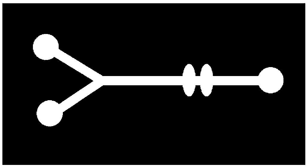
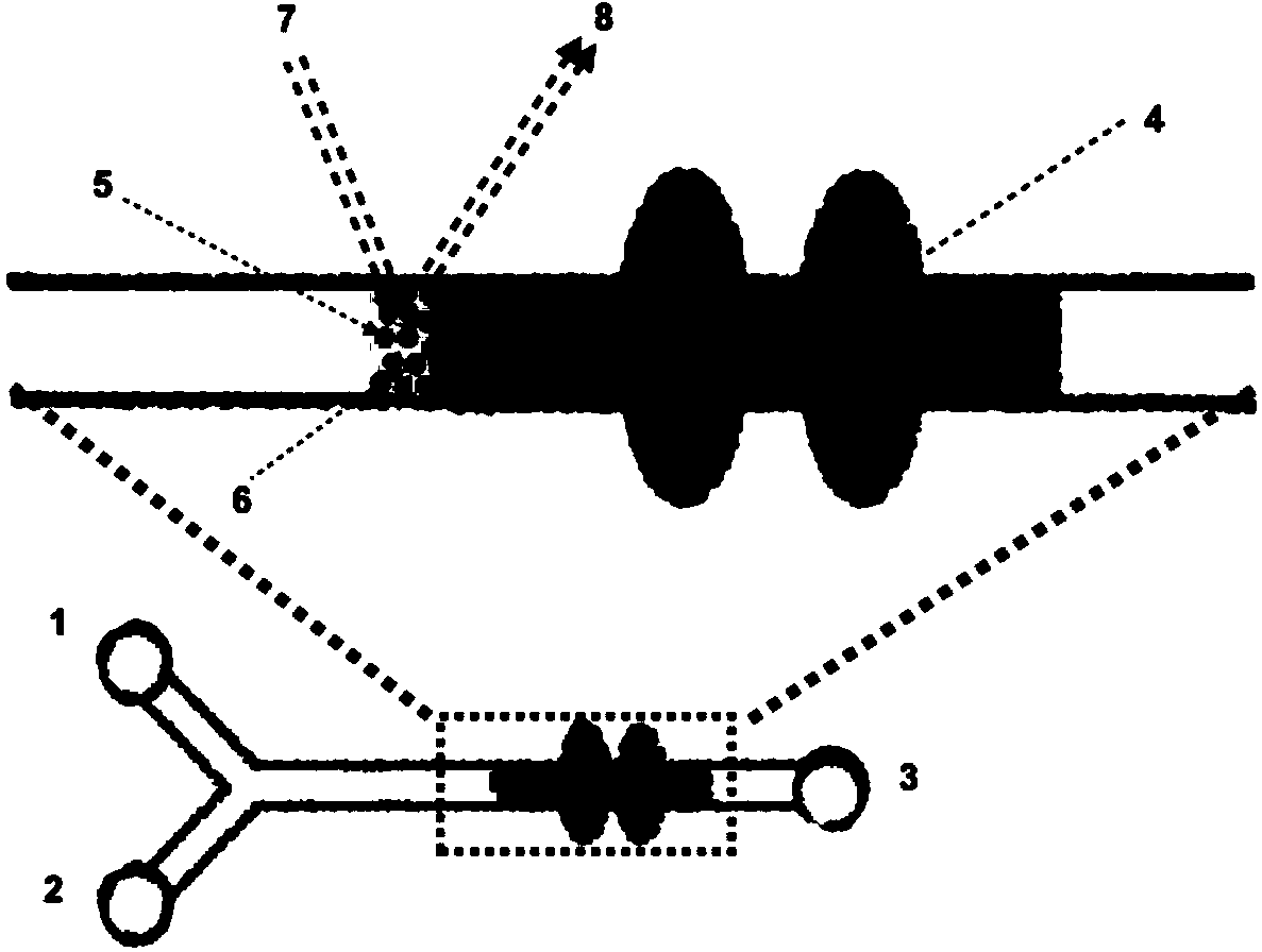
[0041] (a) Use AutoCAD computer drawing software to design the microfluidic pipeline drawing mask, and design two continuous vertical pipeline ellipses at the exposure place of the microfluidic chip, the long axis is 150-400 μm, and the short axis is 50-200 μm. The technology is different from other microfluidic chips, which usually adopt a rectangular pipeline design. The pipeline design is as follows: figure 1 shown.

[0042] (b) Fabrication of PDMS microfluidic chips using soft lithography standard microfabrication techniques.

[0043](c) Preparation of monolithic column solution, mix monomer (GMA), cross-linking agent (EGDMA), and pore-forming agent (DOP) in a weight ratio of 2:1:7, and then add the above-mentioned 2 % photoinitiator (DMPA), prepare a porous monolithic column solution, ultrasonicate the mixture for 5-20 minutes, then pass nitrogen gas into the monolithic column solution for 5-30 minutes to remove oxygen in the solution, and finally place the monolithic co...

Embodiment 2

[0053] (a) Using AutoCAD computer drawing software to design the microfluidic pipeline drawing mask, the pipeline design is as follows figure 1 As shown, the pipeline design of the exposure area of ​​the microfluidic chip is an ellipse with two continuous vertical pipelines, the long axis is 150-400 μm, and the short axis is 50-200 μm. This technology is different from other microfluidic chips that usually use rectangular pipeline design.

[0054] (b) Fabrication of PDMS chips using soft lithography standard microfabrication techniques.

[0055] (c) Preparation of monolithic column solution, mix monomer (GMA), cross-linking agent (EGDMA), and pore-forming agent (DOP) in a weight ratio of 3:2:5, and then add the above-mentioned 4% of the total weight of the mixture A photoinitiator (DMPA) was used to prepare a porous monolithic column solution, and the mixed solution was ultrasonicated for 5-20 minutes, and then nitrogen gas was passed through the monolithic column solution for...

Embodiment 3

[0065] (a) Using AutoCAD computer drawing software to design the microfluidic pipeline drawing mask, the pipeline design is as follows figure 1 As shown, the pipeline design of the exposure place of the microfluidic chip is an ellipse with two continuous vertical pipelines, the long axis is 150-400 μm, and the short axis is 50–200 μm. This technology is different from other microfluidic chips that usually use rectangular pipeline design. .

[0066] (b) Fabrication of PDMS chips using soft lithography standard microfabrication techniques.

[0067] (c) Preparation of the monolithic column solution, mix the monomer (GMA), cross-linking agent (EGDMA), and pore-forming agent (DOP) in a weight ratio of 3:6:11, and then add the above-mentioned 4.5% of the total weight of the mixture % photoinitiator (DMPA), prepare a porous monolithic column solution, ultrasonicate the mixture for 5-20 minutes, then pass nitrogen gas into the monolithic column solution for 5-30 minutes to remove oxy...


PUM

PropertyMeasurementUnit
diameteraaaaaaaaaa
pore sizeaaaaaaaaaa
lengthaaaaaaaaaa

Abstract

The invention provides a preparation method of a microfluidic monolithic column chip and an application of the chip in raman detection. The method comprises the steps that a polydimethylsiloxane (PDMS) microfluidic chip is prepared; a porous monolithic column solution is prepared; a monomer, a crosslinking agent, a pore-forming agent and a photoinitiator are subjected to ultrasonic mixing; nitrogen is supplied for deoxygenization; and finally the monolithic column solution is put in an ice bath for preservation. The solution is injected into a microfluidic chip pipeline, sealed and subjected to ultraviolet exposure, methanol washing is adopted for removing the pore-forming agent and the unreacted monomer, deionized water is used for washing sufficiently, a silver microsphere solution is injected into the microfluidic chip, ultra-sensitive raman real-time detection of a to-be-detected sample is achieved by utilizing silver microsphere enrichment and a surface raman enhancement effect, and a detection limit of the method can reach 10-12M. The method is convenient, flexible, low in cost, low in energy consumption, and convenient to popularize, and is widely applied to the fields of serum marker detection, gas marker detection, environmental monitoring, food safety and the like.

Description

technical field [0001] The invention relates to a preparation method of a microfluidic monolithic column chip, and applies the microfluidic monolithic column chip to Raman detection applications in the fields of organic small molecules, biomedicine, food safety, environmental monitoring, etc., and belongs to material preparation and application field. Background technique [0002] The microfluidic system is a micro-volume liquid (10 -9 –10 -18 L) In the process of manipulation in the pipeline of tens to hundreds of microns, compared with the traditional experimental bench-top technology, the microfluidic device has the following advantages, such as small volume, low reagent consumption, fast analysis, multi-channel detection, etc., however, At present, the development trend of microfluidic devices is becoming more and more complex, and multiple operating units such as separation, mixing, enrichment, and detection are integrated on one chip. In order to realize the multifu...

Claims


Application Information

Patent Timeline
Patent Type & Authority Applications(China)
IPC IPC(8): B81C1/00G01N21/65
Inventor 崔大祥陈守慧王智华
Owner SHANGHAI JIAO TONG UNIV
Learn More