Manufacturing method for bar-type array tellurium-zinc-cadmium detector

A technology for cadmium zinc telluride and detectors, which is applied in the field of preparation of strip array cadmium zinc telluride detectors, can solve the problems of edge defects of lithography images, sag lithography electrode patterns, uneven thickness of wafers, and the like, and saves the preparation. time, overcoming sag, reducing the effect of processing costs

Active Publication Date: 2014-02-05
IMDETEK
View PDF2 Cites 5 Cited by
  • Summary
  • Abstract
  • Description
  • Claims
  • Application Information

AI Technical Summary

Problems solved by technology

[0004] In order to overcome the edge defect problem of the lithographic image when the existing lithography process is used to prepare the CdZnTe detectors in strip arrays, obtain a complete lithography electrode, and facilitate the subsequent flip-chip connection between the CdZnTe detectors in the strip array and the substrate , the invention provides a method for preparing a bar array CdZnTe detector
It overcomes the phenomenon of edge collapse and incomplete photolithographic electrode pattern caused by large aspect ratio during wafer polishing, and solves the short circuit problem caused by uneven wafer thickness during flip-chip connection of pixel electrodes

Method used


Image

  • Manufacturing method for bar-type array tellurium-zinc-cadmium detector
  • Manufacturing method for bar-type array tellurium-zinc-cadmium detector

Examples


Embodiment 1

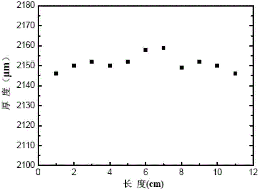
[0017] Step 1: CdZnTe crystal ingot grown by the vertical Bridgman method is oriented along the direction to cut out a size of 12×10mm 2 , a rectangular single wafer with a thickness of 0.5 mm.

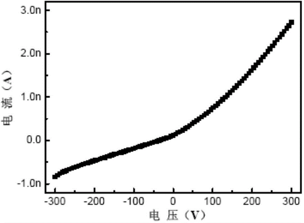
[0018] Step 2: After the wafer is mechanically polished and chemically polished, the Au electrode is evaporated on the {111}Cd surface of the wafer by thermal evaporation, and a photoresist is coated on the electrode to protect the Au electrode from subsequent processing. Destroyed; four 1×8 strip array patterns were simultaneously photolithographically etched on the {111} Te surface of a single wafer, and Au electrodes were prepared by thermal evaporation.

[0019] Step 3: Uniformly coat a layer of photoresist on the surface of the photolithography electrode of the single wafer to protect the strip array electrode from being washed and damaged by the cutting fluid during scribing and cutting. A dicing machine is used to slit along the outer contour of the strip array electrode patt...

Embodiment 2

[0025] Step 1: CdZnTe crystal ingot grown by the vertical Bridgman method is oriented along the direction to cut out a size of 20×20mm 2 , a rectangular single wafer with a thickness of 5 mm.

[0026] Step 2. After the wafer is mechanically polished and chemically polished, AuCl with a concentration of 10-50g / L is used on the {111}Cd surface of the wafer. 3 The Au electrode is prepared by the chemical method of aqueous solution, and the photoresist is evenly coated on the electrode to protect the Au electrode from being damaged in the subsequent processing; six 1×32 pixels are simultaneously photolithographically etched on the {111} Te surface of the wafer Array patterns, and use AuCl with a concentration of 10-50g / L 3 Preparation of Au electrodes by chemical method in aqueous solution.

[0027] Step 3: Uniformly coat a layer of photoresist on the surface of the photolithography electrode of the single wafer to protect the strip array electrode from being washed and damaged...


PUM


Abstract

The invention discloses a manufacturing method for a bar-type array tellurium-zinc-cadmium detector. The manufacturing method is used for solving the technical problem that a photoetching image edge is deficient when an existing method is used for manufacturing a bar-type array tellurium-zinc-cadmium detector. According to the technical scheme, a plurality of bar-type array patterns are made at a time through photoetching on a large-size tellurium-zinc-cadmium single crystal wafer with the small length-width ratio, photoresist is used for protecting a bar-type array electrode, a wafer scriber is used for ripping the peripheral contour of the photoetched patterns, and an independent bar-type tellurium-zinc-cadmium detector is formed. The problems that the turned-down edge is generated and photoetched electrode patterns are incomplete in the wafer polishing process due to the large length-width ratio are solved, and the problem that short circuit is caused due to the wafer with nonuniform thicknesses during the inversion connection of a pixel electrode is solved. Due to the fact that the photoresist is used for protecting the bar-type array electrode to conduct scribing cutting, a photoetched electrode is protected, and wafer edge cracking caused by cutting is avoided. Four to eight 1*8-1*32 pixel array bar-type detectors can be manufactured at a time, and manufacturing cost is reduced.

Description

technical field [0001] The invention relates to a method for preparing a detector, in particular to a method for preparing a bar array CdZnTe detector. Background technique [0002] Due to its large atomic number, cadmium zinc telluride material has high energy resolution and detection efficiency for X or gamma rays with energy in the range of 10keV ~ 1MeV, and has stable performance, no polarization and deliquescent phenomena. At the same time, the cadmium zinc telluride detector can work at room temperature, so the refrigeration system can be omitted, the volume is smaller, and the use is more convenient. However, for CdZnTe detectors with different electrode structures, the strip array structure detector not only overcomes the shortcomings of low efficiency of unit structure detectors, but also overcomes the shortcomings of complex structure and high price of pixel array structure detectors, and has become the current A research hotspot of CdZnTe detectors for X or gamma...

Claims


Application Information

Patent Timeline
Patent Type & Authority Applications(China)
IPC IPC(8): H01L31/18G01T1/24
CPCH01L31/022408H01L31/035281H01L31/1832Y02P70/50
Inventor 徐亚东何亦辉杨波王涛查钢强介万奇
Owner IMDETEK
Why Eureka
Try Eureka