Copper plating solution for PCB (printed circuit board) through holes and PCB blind holes, as well as preparation method and plating method of copper plating solution
A technology of electroplating copper and solution, which is applied in the direction of electrical connection formation of printed components
- Summary
- Abstract
- Description
- Claims
- Application Information
AI Technical Summary
Problems solved by technology
Method used
Image


Examples
Embodiment 1
[0092] A copper electroplating solution for through-hole blind holes of PCB, each component and content thereof of the copper electroplating solution are:
[0093] Copper sulfate pentahydrate: 100g / L
[0094] Sulfuric acid: 100g / L
[0096] Brightener: 5g / L
[0097] Carrier: 3g / L
[0098] Leveling agent: 2g / L
[0099] Deionized water balance;
[0100] And the concentration ratio of copper sulfate pentahydrate to sulfuric acid is 1:1.
[0101] The brightener is a mixture of sodium 3-mercapto-1-propanesulfonate and ethylene thiourea with a weight ratio of 1.5:1; the carrier is made of polyethylene glycol with a molecular weight of 5000 and A mixture of polypropylene glycol in a weight ratio of 1.8:1.
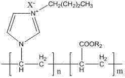
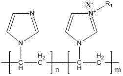
[0102] The leveling agent is a mixture of leveling agent A and leveling agent B with a weight ratio of 1.2:1; wherein, the leveling agent A is a polyvinylimidazolium quaternary ammonium compound, and the leveling agent B is N- Vinyl-N'-butylimid...
Embodiment 2
[0121] A copper electroplating solution for through-hole blind holes of PCB, each component and content thereof of the copper electroplating solution are:
[0122] Copper sulfate pentahydrate: 140g / L
[0123] Sulfuric acid: 120g / L
[0125] Brightener: 15g / L
[0126] Carrier: 10g / L
[0127] Leveling agent: 5g / L
[0128] Deionized water balance;
[0129] And the concentration ratio of copper sulfate pentahydrate to sulfuric acid is 1.17:1.
[0130] The brightener is a mixture of sodium 3-mercapto-1-propanesulfonate and ethylene thiourea in a weight ratio of 2:1; the carrier is made of polyethylene glycol with a molecular weight of 8000 and A mixture of polypropylene glycol in a weight ratio of 2:1.
[0131] The leveling agent is a mixture of leveling agent A and leveling agent B with a weight ratio of 1.5:1; wherein, the leveling agent A is a polyvinylimidazolium quaternary ammonium compound, and the leveling agent B is N- Vinyl-N'-butylimida...
Embodiment 3
[0150] A copper electroplating solution for through-hole blind holes of PCB, each component and content thereof of the copper electroplating solution are:
[0151] Copper sulfate pentahydrate: 220g / L
[0152] Sulfuric acid: 180g / L
[0154] Brightener: 35g / L
[0155] Carrier: 20g / L
[0156] Leveling agent: 15g / L
[0157] Deionized water balance;
[0158] And the concentration ratio of copper sulfate pentahydrate to sulfuric acid is 1.22:1.
[0159] The brightener is a mixture of sodium 3-mercapto-1-propanesulfonate and ethylene thiourea with a weight ratio of 2.5:1; the carrier is made of polyethylene glycol with a molecular weight of 10000 and A mixture of polypropylene glycol in a weight ratio of 2.2:1.
[0160]The leveling agent is a mixture of leveling agent A and leveling agent B with a weight ratio of 1.8:1; wherein, the leveling agent A is a polyvinylimidazolium quaternary ammonium compound, and the leveling agent B is N- Vinyl-N'-but...
PUM
 Abstract
Description
Claims
Application Information
 - R&D
- Intellectual Property
- Life Sciences
- Materials
- Tech Scout
- Unparalleled Data Quality
- Higher Quality Content
- 60% Fewer Hallucinations
Browse by: Latest US Patents, China's latest patents, Technical Efficacy Thesaurus, Application Domain, Technology Topic, Popular Technical Reports.
© 2025 PatSnap. All rights reserved.Legal|Privacy policy|Modern Slavery Act Transparency Statement|Sitemap|About US| Contact US: help@patsnap.com