Method for preparing nanoscale thickness thin film and structure on curved surface substrate

A nano-structure and nano-scale technology, which is applied to the photo-engraving process, opto-mechanical equipment, optics and other directions of the pattern surface, can solve the problem of inability to form a uniform nano-thick film, and achieve the effect of simple equipment requirements and low cost.

Active Publication Date: 2014-02-12
WUXI IMPRINT NANO TECH
View PDF5 Cites 13 Cited by
  • Summary
  • Abstract
  • Description
  • Claims
  • Application Information

AI Technical Summary

Problems solved by technology

Traditional adhesive coating methods such as spin coating, spray coating, and dip coating can

Method used


Image

  • Method for preparing nanoscale thickness thin film and structure on curved surface substrate
  • Method for preparing nanoscale thickness thin film and structure on curved surface substrate

Examples


Embodiment Construction

[0023] The present invention will be described in further detail below in conjunction with the accompanying drawings and embodiments.

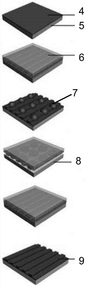
[0024] (1) Preparation of composite nanoimprint template

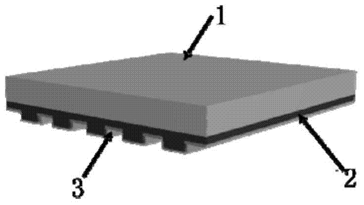
[0025] Use elastic polydimethylsiloxane (PDMS) to absorb a layer of UV-curable glue (UV-resist), then cover it on the master template with nanostructures and send it to exposure treatment under ultraviolet light, and the exposure is completed Finally, a rigid nanostructure layer was formed on the elastic PDMS surface, and then a low surface energy monolayer (1H, 1H, 2H, 2H-perfluorodecyltrichlorosilane) was grown on the structure as Anti-adhesive layer, the composite template 6 that can be used repeatedly like this is just done. The structure of composite template 6 is as follows figure 1 As shown, the rigid structure layer is a grating structure with a period of 550 nm and a depth of 110 nm.

[0026] (2) Spin coating

[0027] On a clean silicon wafer 5, evenly coat a layer of 400-...


PUM

PropertyMeasurementUnit
Thicknessaaaaaaaaaa
Thicknessaaaaaaaaaa

Abstract

The invention belongs to the technical field of nanometric machining, and specifically relates to a method for preparing a nanoscale thickness thin film and structure on a curved surface substrate. The method comprises the steps of (1) preparing a composite nanometer impressing template which is reused many times; (2) coating a layer of ultraviolet light polymerization glue on a silicon slice; (3) attaching the composite nanometer impressing template to the silicon slice with the glue layer, adsorbing for a while, separating the composite template from the silicon slice, and contacting the composite template with the ultraviolet light polymerization glue and a target substrate which needs embossing, thus forming the uniform liquid film by liquid drops between the composite template and the target substrate; and (4) carrying out ultraviolet exposure on the structure, and separating the template and the substrate after finishing the exposure so as to obtain the nanostructure, wherein the nanostructure and the composite template are complementary. The method provided by the invention utilizes the composite nanometer impressing template to transfer the glue layer, and thus that the uniform nanoscale thickness thin film is formed on the surface of a non-planar substrate or a high curvature substrate.

Description

technical field [0001] The invention belongs to the field of micro-nano processing, and in particular relates to a method for preparing a nano-scale thin film and structure on a curved substrate in a double-transfer manner. Background technique [0002] In recent years, the preparation of nanoscale structures on curved and complex surfaces has attracted widespread attention, especially in image sensing arrays, artificial compound eyes, fiber optic sensors and other fields. The existing micro-nano-fabrication technology represented by photolithography is not up to the requirements of preparing patterns on non-planar substrates. Therefore, a low-cost, high-quality preparation method for curved surface nanopatterns is urgently needed to be developed. [0003] Nanoimprinting is a pattern replication technology developed in the mid-1990s. It has the advantages of high resolution, high output, and low cost. Among them, UV-curable nanoimprinting technology has been widely used in ...

Claims


Application Information

Patent Timeline
IPC IPC(8): G03F7/00
Inventor 钱明成袁长胜
Owner WUXI IMPRINT NANO TECH
Why Eureka
Try Eureka