Electric field aided silicon through hole etching process

An electric field-assisted, through-silicon via technology, which is applied in the manufacture of circuits, electrical components, semiconductors/solid-state devices, etc., can solve problems such as affecting surface quality, difficulty in etching through holes, and difficulty in achieving deep etching of micron-scale patterns.

Inactive Publication Date: 2013-03-06
HUAZHONG UNIV OF SCI & TECH
View PDF6 Cites 19 Cited by
  • Summary
  • Abstract
  • Description
  • Claims
  • Application Information

AI Technical Summary

Problems solved by technology

The smoothness and verticality of the side wall are not ideal
In addition, it takes hundreds of cycles to etch through holes by using the above process, and the photoresist will be damaged, which makes it difficult to protect the surface of the silicon wafer and affect the surface quality.
In addition, ICP equipment and etching gas are very expensive, which is not conducive to the popularization and application of this technology
[0004] In recent years, the metal-catalyzed etching process has developed rapidly. Using a single noble metal particle or film can achieve deep etching of nanoscale patterns, but it is still very difficult to achieve through-hole etching, and it is difficult to achieve deep etching of micron-scale patterns.

Method used


Image

  • Electric field aided silicon through hole etching process
  • Electric field aided silicon through hole etching process
  • Electric field aided silicon through hole etching process

Examples


Embodiment 1

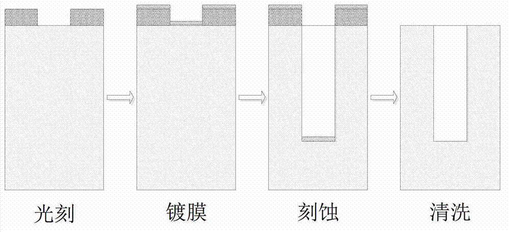
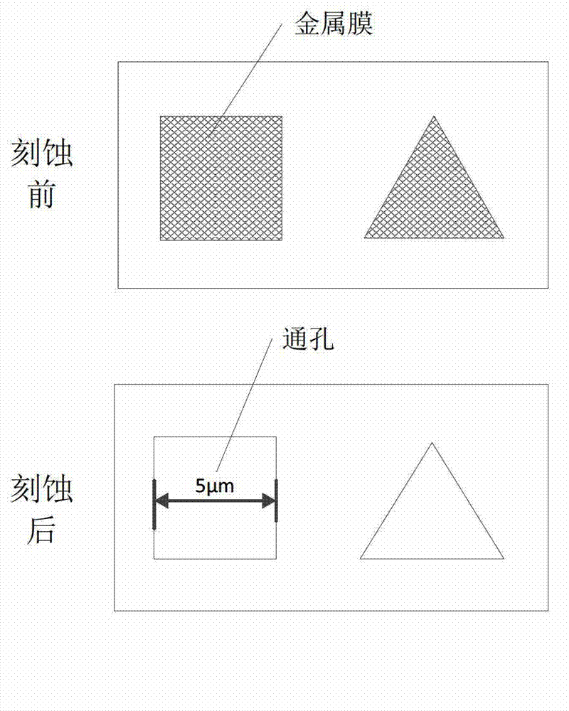
[0027] see figure 1 and figure 2 , figure 1 It is a process block diagram of the inventive method. figure 2 It is a schematic diagram of the through-hole structure made according to Embodiment 1 of the present invention, such as figure 1 and figure 2 As shown in , the electric field-assisted TSV metal-catalyzed etching process in this example includes the following specific steps:

[0028] (a) Clean the single crystal silicon wafer, then spin-coat photoresist on its surface, and transfer the micron-scale pattern on the mask corresponding to the square hole and triangular hole structure with the required characteristic size of 5 microns by photolithography process onto the photoresist, thereby forming a photoresist pattern with micron holes.

[0029] (b) On the single crystal silicon wafer formed with the above-mentioned photoresist with micron holes, a 40nm gold film is plated by using a magnetron sputtering process.

[0030] (c) Using HF, H 2 o 2 The mixed solution...

Embodiment 2

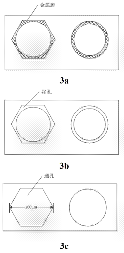
[0034] see figure 1 and image 3 , image 3 It is a schematic diagram of the structure of the large-sized through hole prepared according to the second embodiment of the present invention. Its specific manufacturing process steps include:

[0035] (a) Clean the single crystal silicon wafer, then spin-coat photoresist on its surface, and transfer the ring-like pattern with a diameter of about 200 microns on the mask to the photoresist by photolithography process, thereby forming a micron Photoresist pattern for ring holes.

[0036] (b) On the single-crystal silicon wafer formed with the above-mentioned micron ring holes, a 50nm silver film is plated by electron beam evaporation process.

[0037] (c) Using HF, H 2 o 2 The mixed solution of deionized water and deionized water is used as an etchant to carry out metal-catalyzed etching on a single crystal silicon wafer. The etching reaction is in an electric field with a strength of 500v / m, and the direction of the electric f...

Embodiment 3

[0041] see figure 1 and Figure 4 , Figure 4 It is a schematic diagram of the structure of the nanoscale through-hole array prepared according to the third embodiment of the present invention. Its specific manufacturing process steps include:

[0042] (c) Clean the single crystal silicon wafer, then spin-coat photoresist on its surface, and form a photoresist pattern corresponding to the 50 nanometer hole array by electron beam lithography.

[0043] (d) On the single crystal silicon wafer formed with the above-mentioned nanohole photoresist pattern, a 20nm silver film was plated by using a magnetron sputtering process.

[0044] (c) Using HF, H 2 o 2 A mixed solution of deionized water and deionized water is used as an etchant to carry out metal-catalyzed etching on a single crystal silicon wafer. The etching reaction is in an electric field with a strength of 10v / m, and the direction of the electric field is perpendicular to the surface of the silicon wafer. The mixed so...


PUM


Abstract

The invention discloses an electric field aided silicon through hole etching process. The process comprises the following steps of (1) spinning a photoresist on a monocrystalline wafer and performing optical lithography or electron-beam lithography to obtain a photoresist pattern; (2) plating a silver film or a golden film; (3) in an electric field, taking a mixed solution of HF, H2O2 and deionized water as an etching agent to perform metal catalytic etching; (4) removing the photoresist; and (5) removing the residual metal film on the monocrystalline wafer and cleaning the monocrystalline wafer. Through hole structures with various micro nanometer sizes from tens of nanometer to hundreds of nanometer are formed by controlling the strength of the electric field in the etching process.

Description

technical field [0001] The invention relates to the field of micro-nano manufacturing, and more specifically, to an electric-field-assisted through-silicon via metal catalytic etching process. Background technique [0002] With the rapid development of electronic information, automotive electronics, aerospace and other industries, higher requirements are placed on the processing and packaging of micro-electromechanical systems and micro-fluidic systems. Three-dimensional integrated electronic packaging needs to make many through holes on the silicon chip to realize the electrical interconnection between different chips. Various fluidic channels are required in microfluidic systems. Therefore, through-silicon via etching technology has become an important technology in the field of micro-nano manufacturing. [0003] The TSV etching technology is essentially a deep silicon etching technology. At present, deep silicon etching generally uses ICP equipment and adopts Bosch pro...

Claims


Application Information

Patent Timeline
Patent Type & Authority Applications(China)
IPC IPC(8): H01L21/768
CPCH01L21/76898
Inventor 廖广兰史铁林孙博盛文军张康汤自荣夏奇高阳谭先华
Owner HUAZHONG UNIV OF SCI & TECH
Why Eureka
Try Eureka