A method of degumming after high-energy ion implantation

An ion implantation, high-energy technology, applied in electrical components, semiconductor/solid-state device manufacturing, circuits, etc., can solve problems such as adverse effects on devices, affect device performance, and difficult to remove, reduce wafer surface defects, and improve product quality. rate, the effect of reducing the generation of residues

Active Publication Date: 2016-08-17
SHANGHAI HUALI MICROELECTRONICS CORP
View PDF5 Cites 0 Cited by
  • Summary
  • Abstract
  • Description
  • Claims
  • Application Information

AI Technical Summary

Problems solved by technology

However, for some special products and graphics, there will still be defects using the above method. Such defects are mainly C-Si-O residues, which are difficult to remove in subsequent wet cleaning;
[0010] 3. Use CF 4 Reactive gas can effectively remove C-Si-O residues and surface hard shells, but it will have other adverse effects on the device
due to CF 4 The gas has strong etching and corrosiveness, which will bring new etching damage to the oxide film or nitride film on the side wall of polysilicon, the silicon or oxide film substrate, and cause the critical dimension of the device or the amount of damage to the substrate silicon. change, which affects the performance of the device

Method used


Image

  • A method of degumming after high-energy ion implantation
  • A method of degumming after high-energy ion implantation
  • A method of degumming after high-energy ion implantation

Examples


Embodiment Construction
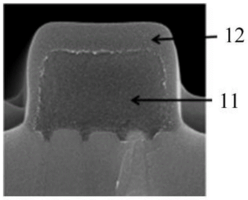
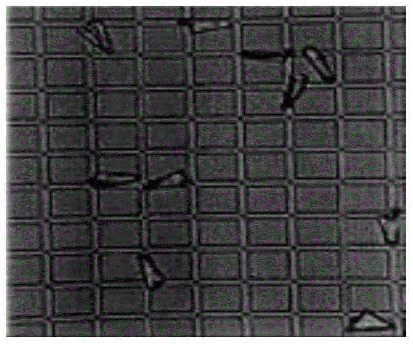
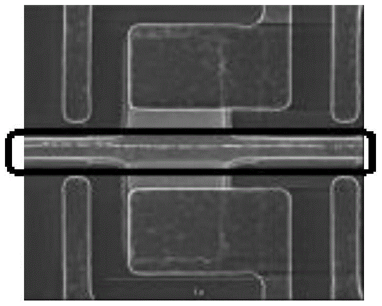
[0032] The core idea of ​​the present invention is to propose a degumming method after high-energy ion implantation, which adopts three stages of degumming, the first stage is the wafer preheating stage, and the process temperature required for subsequent reactions is reached; the second stage It is the surface hard shell removal stage, using pure hydrogen and nitrogen mixed gas as the process gas to remove the surface carbonized hard shell after high-energy ion implantation; the third stage is the main photoresist removal stage, mixed with a certain proportion of oxygen, hydrogen, nitrogen Gas is the process gas to remove residual photoresist. The degumming method of the three-stage process of the present invention utilizes the principle of hydrogen to reduce the cross-linked carbon chain, and removes the carbonized hard shell on the outer surface of the photoresist after injection under mild reaction conditions, thereby avoiding the excessive degumming rate at the beginning o...


PUM


Abstract

The invention provides a method for removing photoresist after high-energy ion implantation. Three stages are adopted to remove the photoresist. The first stage is a wafer preheating stage, and the process temperature required by consequent reactions is reached. The second stage is a surface shell removing stage, and combination gas of pure hydrogen and nitrogen is applied as process gas to remove surface carbonization shells after the high-energy ion implantation. The third stage is a body photoresist removing stage, and combination gas of oxygen, hydrogen and nitrogen with a certain proportion is used as process gas to remove the remaining photoresist. According to the method for removing the photoresist through the three-stage processes, on the basis of the principle that hydrogen reduces cross-linked carbon chains, the carbonization shells on the outer surface of the photoresist are firstly removed after the implantation under the mild reaction condition, and therefore the phenomenon that due to the fact that the photoresist removing speed is excessively high at the reaction beginning stage, the photoresist bursts is prevented from happening. Meanwhile, residue generation containing carbon silicon dioxide in the reaction process is reduced, additional damage to other membranes is not caused, defects on the surfaces of wafers are effectively reduced, and the product yield is improved.

Description

technical field [0001] The invention relates to the field of semiconductor manufacturing, in particular to a method for removing glue after high-energy ion implantation. Background technique [0002] In the front-end process of semiconductor wafer production, plasma dry stripping is widely used in the removal process of residual photoresist after high-energy ion implantation. After the wafer has been processed by photoresist coating, exposure, development and other processes, after high-energy ion implantation, the exposed pattern is the area that needs to be ion implanted according to the electrical characteristics of the product. At the same time, the surface of the area covered by photoresist (which is Figure 1A As shown in 11, the photoresist that has not been infiltrated) will form a hard surface crust (crust) with a certain thickness (such as Figure 1A hard shell as shown in 12). The hard shell 12 is mainly composed of cross-linked carbon chain compounds and doped w...

Claims


Application Information

Patent Timeline
Patent Type & Authority Patents(China)
IPC IPC(8): H01L21/3105G03F7/42
CPCG03F7/42H01L21/31138
Inventor 荆泉高腾飞任昱吕煜坤张旭升
Owner SHANGHAI HUALI MICROELECTRONICS CORP
Why Eureka
Try Eureka