A kind of LED epitaxial wafer and preparation method thereof

A technology of LED epitaxial wafers and vapor phase epitaxy, which is applied in the direction of semiconductor devices, electrical components, circuits, etc., can solve the problems of low LED luminous efficiency, increased device voltage, increased heat generation, etc., to improve ESD performance, easy to implement, The effect of enhancing current uniformity

Active Publication Date: 2016-08-17
BYD SEMICON CO LTD
View PDF5 Cites 0 Cited by
  • Summary
  • Abstract
  • Description
  • Claims
  • Application Information

AI Technical Summary

Problems solved by technology

[0005] In order to solve the technical problems that the LED epitaxial wafers in the prior art are unsatisfactory in improving the ESD performance, which easily lead to an increase in the voltage of the device, increase in heat generation, and the luminous efficiency of the LED is not high, the present invention provides a method that can effectively improve the ESD performance. performance, and the enhanced luminous efficiency improves the brightness of the LED, does not introduce defects, and does not cause the increase of the series resistance to deteriorate the electrical properties of the device, and the LED epitaxial wafer with a simple production process and its preparation method

Method used


Image

  • A kind of LED epitaxial wafer and preparation method thereof

Examples


preparation example Construction

[0027] The present invention also provides a method for preparing the above-mentioned LED epitaxial wafer, comprising: sequentially growing a first semiconductor layer, an insertion layer, a light-emitting layer, and a second semiconductor layer on a substrate layer, wherein the step of growing the insertion layer includes using a vapor phase epitaxy growth method Using trimethylgallium as gallium source, ammonia as nitrogen source, GeH 4 A Ge-doped GaN layer is grown on the first semiconductor layer as a dopant source.

[0028] The vapor phase epitaxial growth method refers to the growth by metal organic chemical vapor deposition (MOCVD method), and the epitaxial lateral growth of different sizes is realized by controlling the pressure, temperature, gas flow ratio and reaction time in the reaction chamber.

[0029] Preferably, the growth temperature for growing the Ge-doped GaN layer is 900-1100°C. H 4 The flow rate of the gas is 1~10 sccm; the flow rate of trimethylgallium...

Embodiment 1

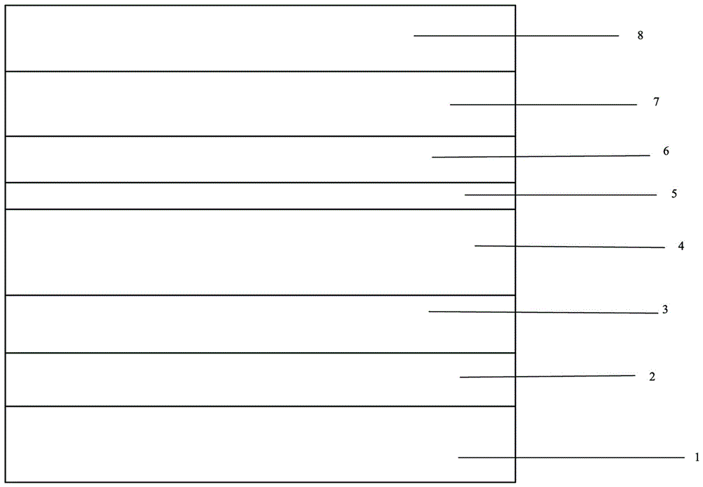
[0058] Pure hydrogen gas (H 2 ) as the carrier gas, the schematic diagram of the prepared sample structure is shown in figure 1 .

[0059] (1) Using sapphire as the substrate layer 1, using NH by MOCVD 3(The flow rate is 20000sccm) Nitriding treatment is first performed on the sapphire substrate layer 1 at 530°C for 150s, and then TMGa (flow rate is 75sccm) is passed through for 140s to deposit a GaN layer with a thickness of about 30nm on the sapphire substrate layer 1, and then go through a high temperature of 1070°C After processing for 270s, a buffer layer 2 is formed on the substrate layer.

[0060] (2) At a temperature of 1050 °C, TMGa (flow rate of 220 sccm) and NH 3 (The flow rate is 36000sccm) as the source, grow for 3800s, and grow a 2 μm non-doped GaN layer 3 on the buffer layer 2 .

[0061] (3) At a temperature of 1050 ° C, TMGa (flow rate of 270 sccm) and NH 3 (The flow rate is 36000sccm) as the source, while using SiH 4 (The flow rate is 6 sccm) for the dop...


PUM


Abstract

The invention provides an LED epitaxial wafer and a preparing method thereof. The LED epitaxial wafer comprises a substrate layer, a first semiconductor layer, an interpolating layer, a light-emitting layer and a second semiconductor layer, wherein the substrate layer, the first semiconductor layer, the interpolating layer, the light-emitting layer and the second semiconductor layer are sequentially stacked. The interpolating layer is a GE doping GaN layer, ESD performance can be effectively improved, lighting efficiency is intensified, the brightness of an LED is improved, defects are not generated, the situation that the electrical property of a component becomes poor due to increase of serial-connection resistors cannot occur, and meanwhile the production process is simple.

Description

technical field [0001] The invention belongs to the field of semiconductor lighting, in particular to an LED epitaxial wafer and a preparation method thereof. Background technique [0002] Group III-V nitride materials based on gallium nitride (GaN), indium gallium nitride (InGaN), aluminum gallium nitride (AlGaN) and indium aluminum gallium nitride (AlGaInN) have continuously adjustable direct bandwidth of 0.7-6.2eV, covering a wide spectral range from ultraviolet to infrared, it is an ideal material for manufacturing blue, green and white light-emitting devices. The structure of the existing LED epitaxial wafer is generally: a layer of n-type GaN layer is epitaxially grown on a surface of a sapphire substrate layer, and a light-emitting layer is grown on the side of the n-type GaN layer opposite to the surface of the substrate layer, and the light-emitting layer is opposite to the surface of the substrate layer. A p-type GaN layer is grown on one side of the surface of th...

Claims


Application Information

Patent Timeline
Patent Type & Authority Patents(China)
IPC IPC(8): H01L33/14H01L33/00
CPCH01L33/0075H01L33/14
Inventor 陈飞
Owner BYD SEMICON CO LTD
Why Eureka
Try Eureka