

Method for fabricating patterned sapphire substrate by nanoimprint technology without residual layer
A patterned sapphire and nano-imprinting technology, which is applied in the direction of optomechanical equipment, photo-plate making process of pattern surface, optics, etc., can solve the problems of nano-imprinting residual layer, etc., and achieve industrialization, short process, and pattern resolution high rate effect
- Summary
- Abstract
- Description
- Claims
- Application Information
AI Technical Summary
Problems solved by technology
Method used
Image

Examples
specific Embodiment approach
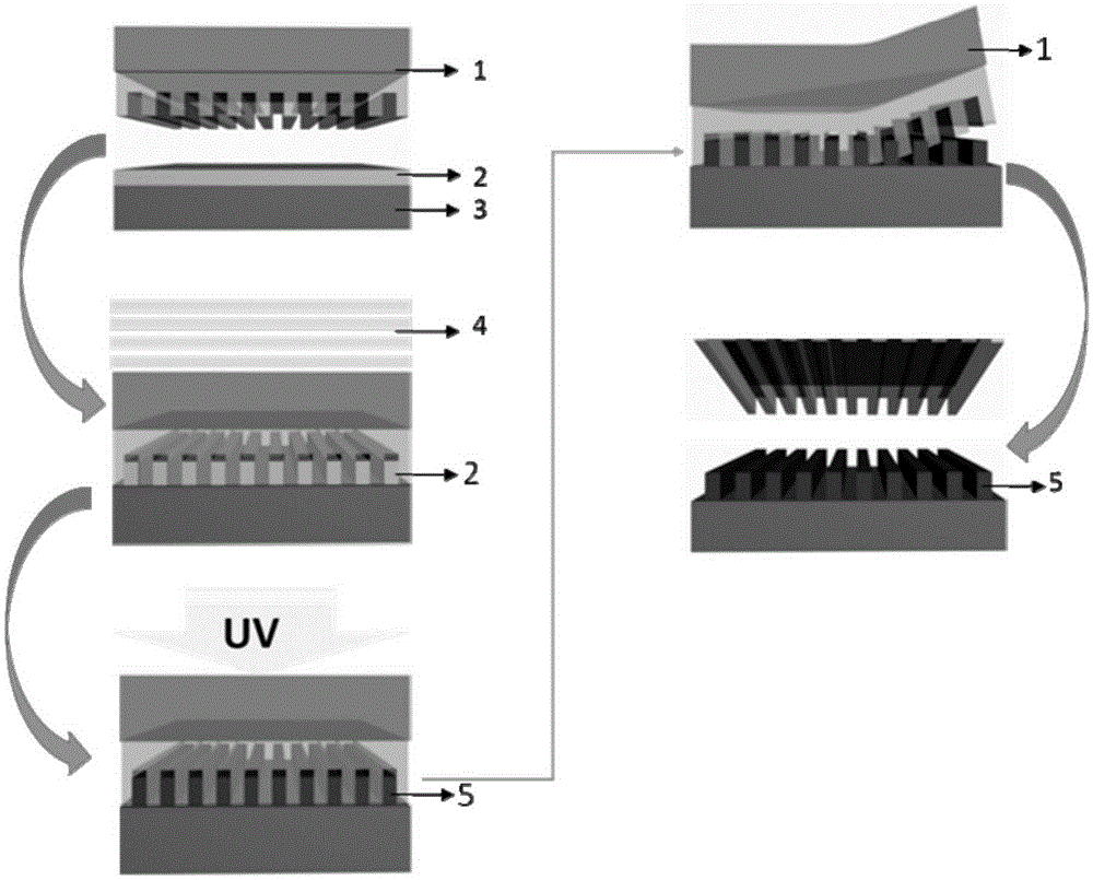
[0024] (1) Anti-adhesive treatment of composite formwork
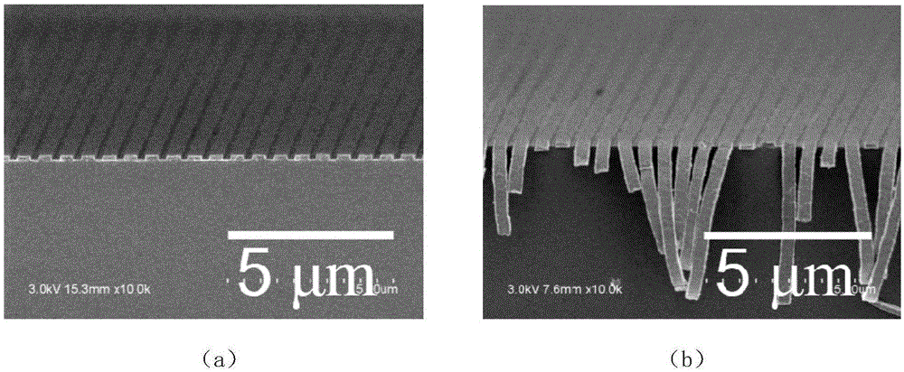
[0025] Select a grating composite template with a period of 550nm and a depth of 110nm, and perform oxygen plasma treatment on the surface of the composite template for a very short time, so that a very thin layer of silicon dioxide is formed on the surface of the rigid structure layer, and then passed through the anti-adhesive agent in the vacuum desiccator Anti-adhesive treatment of composite formwork by gasification method.
[0026] (2) Selection and control of embossing film thickness
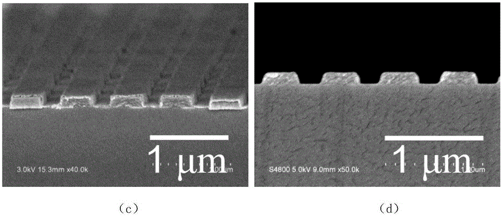
[0027] For the calculation of the duty cycle of the composite template, the depth of the template used is 110nm, the duty ratio is 1:1, the film thickness of the suitable imprinting glue is 55nm, the experimental control film thickness is between 50nm-55nm, and BYK3570 ultraviolet light is selected Take curing glue as an example, the concentration of the glue used is 2%, the speed of glue application is 3000rpm, the time of glue ap...
PUM
| Property | Measurement | Unit |
|---|---|---|
| contact angle | aaaaa | aaaaa |
Abstract
Description
Claims
Application Information