

Top emission organic light-emitting device and manufacturing method thereof
A technology of electroluminescence and top emission, which is applied in the manufacture of semiconductor/solid-state devices, electric solid-state devices, electrical components, etc. It can solve the problem of not considering the change of viewing angle, and achieve the effect of avoiding the change.
- Summary
- Abstract
- Description
- Claims
- Application Information
AI Technical Summary
Problems solved by technology
Method used
Image

Examples
preparation example Construction
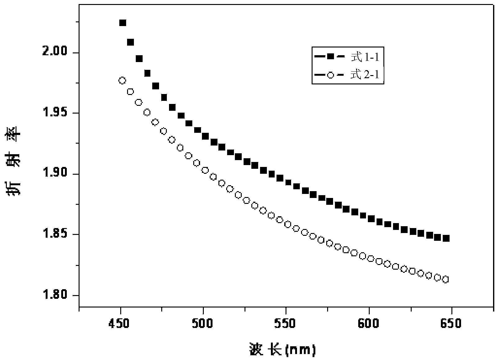
[0105] The preparation method of formula 2-1~2-5 compound is as follows:
[0106]
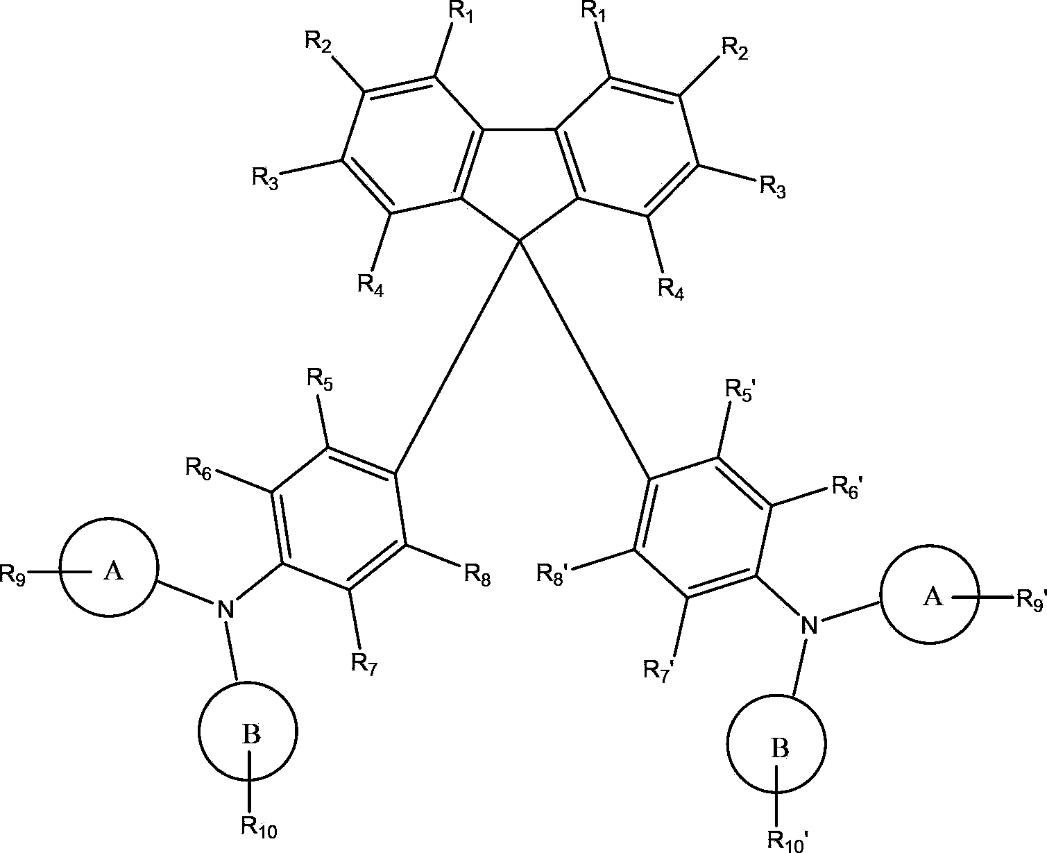
[0107] Under nitrogen protection, 7.4 grams of bis(o-bromophenyl)dimethylsilane (see J.Organomet.Chem.1984,271,319-326 for the synthesis method) (20mmol) was added to a 500ml three-necked flask, and 150ml of anhydrous ether was added dissolve. Cool the reaction system to -80°C, slowly add 1.5M tert-butyllithium (59ml, 88mmol) dropwise, keep the reaction mixture at -80°C during the dropwise addition, continue to stir at this temperature for 1 hour after the dropwise addition is complete . Then add 3.65g benzophenone (20mmol), stir at low temperature for 30 minutes, then remove the cold bath, let the reaction system warm up to room temperature naturally, and continue to stir at room temperature for 3 hours. The reaction was quenched by adding saturated ammonium chloride solution, the product was extracted with ethyl acetate, and the organic phase was dried over anhydrous magnesium sulfate. ...
Embodiment 1
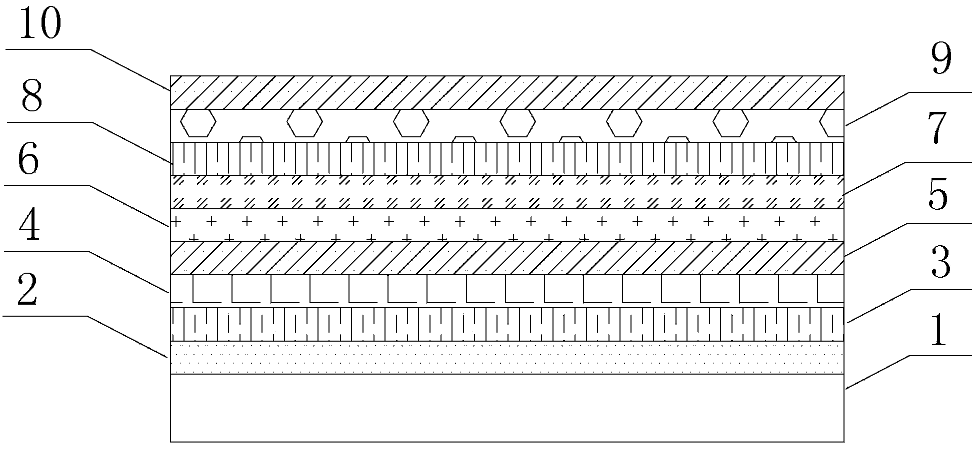
[0135] Ag was sputtered on the glass substrate as a reflective layer with a thickness of 150 nm, ITO was sputtered at 10 nm as the anode of the device, and the desired pattern was etched with O 2 Plasma treatment for 3 minutes. The resulting substrate was placed in vacuum, and 130 nm of a mixture of MTDATA and F4TCNQ was deposited by co-evaporation as a hole injection layer (HIL), where the weight of F4TCNQ was 4% by weight of MTDATA. Next, 10 nm of NPB was deposited as a hole transport layer (HTL). A 30 nm mixture of ADN and DPAVB was then co-evaporated as a light-emitting layer, where the weight of DPAVB was 5% of that of AND. Then 20 nm of Bphen was deposited as the electron transport layer (ETL). Keeping the degree of vacuum constant, through Li 3 During the evaporation process (temperature 600 °C), N was decomposed by evaporating 1 nm of Li as the electron injection layer (EIL), 20 nm of Ag as the cathode, and 40 nm of the organic material with the structure of formula...
Embodiment 2
[0141] Ag was sputtered on the glass substrate as a reflective layer with a thickness of 150 nm, ITO was sputtered at 10 nm as the anode of the device, and the desired pattern was etched with O 2 Plasma treatment for 3 minutes. The resulting substrate was placed in a vacuum, and 170 nm of a mixture of MTDATA and F4TCNQ was deposited by co-evaporation as a hole injection layer (HIL), where the weight of F4TCNQ was 4% by weight of MTDATA. Next, 10 nm of NPB was deposited as a hole transport layer (HTL). A mixture of CBP and Ir(ppy)3 of 30 nm was then co-evaporated as the light-emitting layer, where Ir(ppy) 3 The weight is 5% of the CBP weight. Then 20 nm of Bphen was deposited as the electron transport layer (ETL). Keep the vacuum constant, by KBH 4 During the evaporation process (temperature 400 °C), 1 nm of K was deposited as the electron injection layer (EIL), 20 nm of Ag was deposited as the cathode, and 40 nm of organic material with the structure of formula 1-3 was dep...
PUM
| Property | Measurement | Unit |
|---|---|---|
| Thickness | aaaaa | aaaaa |
| Thickness | aaaaa | aaaaa |
| Thickness | aaaaa | aaaaa |
Abstract
Description
Claims
Application Information