Electrical programming-ultraviolet light erasing memory device structure and preparation method thereof

A storage device and ultraviolet light technology, which is applied in the direction of electrical solid-state devices, semiconductor/solid-state device manufacturing, electrical components, etc., can solve the problem of low device erasing efficiency, improve erasing efficiency and working speed, expand application space, Possibility-enhancing effects

Inactive Publication Date: 2014-02-26
FUDAN UNIV
View PDF2 Cites 14 Cited by
  • Summary
  • Abstract
  • Description
  • Claims
  • Application Information

AI Technical Summary

Problems solved by technology

[0004] Based on the above background, in order to solve the problem of low device erasing efficiency, the present invention proposes an electrical programming-ultraviolet light erasing non-volatile TFT memory structure and its preparation method, that is, the device is erased by ultraviolet light irradiation. remove

Method used


Image

  • Electrical programming-ultraviolet light erasing memory device structure and preparation method thereof
  • Electrical programming-ultraviolet light erasing memory device structure and preparation method thereof
  • Electrical programming-ultraviolet light erasing memory device structure and preparation method thereof

Examples


Embodiment 1

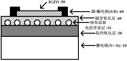
[0068] Step 1: Select a heavily doped N-type single crystal silicon wafer with a resistivity of 0.008~0.100 Ω·cm as the substrate, and clean the silicon wafer through a standard RCA cleaning process, and then remove the surface of the silicon wafer with hydrofluoric acid oxide layer.

[0069] Step 2: On the cleaned silicon wafer, use ALD method to deposit and grow Al 2 o 3 The thin film acts as a blocking oxide layer for the memory. al 2 o 3 The thickness of the film is 20~150nm; during the deposition process, the substrate temperature is controlled between 100~300 ℃; 2 o 3 The reaction sources are trimethylaluminum and water vapor.

[0070] Step 3: Using ALD method on Al 2 o 3 A layer of Pt nanocrystals is deposited on the film as the charge trapping layer of the memory. The reaction sources for the deposition of Pt nanocrystals are (MeCp)Pt(Me)3 and O 2 , the deposition temperature is 200~400°C, and the number of deposition cycles is 10~100.

[0071] Step 4: Depos...

Embodiment 2

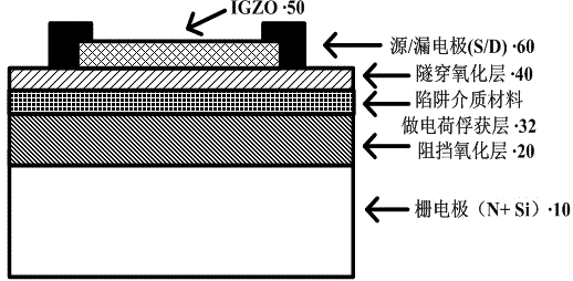
[0081] Step 1: Select a heavily doped N-type single crystal silicon wafer with a resistivity of 0.008~0.100 Ω·cm as the substrate, and clean the silicon wafer through a standard RCA cleaning process, and then remove the surface of the silicon wafer with hydrofluoric acid oxide layer.

[0082] Step 2: On the cleaned silicon wafer, use ALD method to deposit and grow Al 2 o 3 The thin film acts as a blocking oxide layer for the memory. al 2 o 3 The thickness of the film is 20~150nm; during the deposition process, the substrate temperature is controlled between 100~300°C; the growth of Al 2 o 3 The reaction sources are trimethylaluminum and water vapor.

[0083] Step 3: Using ALD method on Al 2 o 3 A layer of ZnAlO film with a thickness of 10-50nm is deposited on the film as the charge trapping layer of the memory. The reaction sources for depositing ZnAlO thin films are trimethylaluminum, diethylzinc and water vapor, and the deposition temperature is 100~300°C. During ea...


PUM


Abstract

The invention provides an electrical programming-ultraviolet light erasing memory device structure and a preparation method thereof. A heavily-doped N type monocrystalline silicon wafer is used as a substrate and an extraction electrode of a gate; an oxide insulator with relatively good compactness is used as a charge barrier layer of a memory; a thin-film material with many charge defects or nanocrystalline is used as a charge capture layer; an oxide insulator with relatively good compactness and a forbidden band being large in width as a tunneling layer of the memory; an IGZO film is used as an electroconductive channel of the memory, an active area is defined through photoetching and wet etching and the electroconductive channel is formed; processing of a source electrode and a drain electrode is completed through photoetching, metal deposition and stripping technology; in test, a positive pulse is applied to a gate electrode to realize programming operation of the device; and erasure of the device is realized by using ultraviolet light to irradiate the device without applying any bias voltage. The electrical programming-ultraviolet light erasing memory device structure solves the problem that an IGZO channel-based TFT memory cannot be erased; the erasure efficiency and the working speed of the device are improved; and the application space of the IGZO channel-based TFT memory is enlarged.

Description

technical field [0001] The invention relates to the technical field of semiconductor integrated circuits, and proposes a structure and a preparation method of an electric programming-ultraviolet light erasing memory for a non-volatile fast flash memory. Background technique [0002] System Panel (SOP) technology integrates various functional components on the same display panel to obtain a high-performance and low-cost system. It is used in the fields of automobiles, computers, consumer electronics, military electronics, wireless communications, and food testing It has important application prospects. As an important component in SOP, non-volatile thin-film transistor (TFT) memory can not only be used for circuit-level adjustment and voltage modification, but also suitable for large-capacity storage of complex display parameters, etc. In the future, pixel storage and storage blocks are also expected to be directly Integrated on the display board, it can not only realize dat...

Claims


Application Information

Patent Timeline
Patent Type & Authority Applications(China)
IPC IPC(8): H01L29/792H01L29/51H01L21/336
CPCH10B43/00H10B43/30
Inventor 丁士进崔兴美陈笋
Owner FUDAN UNIV
Why Eureka
Try Eureka