Circuit for solving inconsistency of gains among batches of chips

A batch-to-batch, consistent technology, applied in gain control, electrical components, amplification control, etc., can solve problems such as unfavorable system integration, complex circuit structure, increase system power consumption, etc. Strong operability without affecting system noise and stability

Active Publication Date: 2014-02-26
CHINA ELECTRONIC TECH GRP CORP NO 38 RES INST
View PDF6 Cites 0 Cited by
  • Summary
  • Abstract
  • Description
  • Claims
  • Application Information

AI Technical Summary

Problems solved by technology

The first is the combination of variable gain amplifier and automatic gain control circuit, through the automatic detection circuit composed of on-chip operational amplifier, feedback circuit and comparator, stable gain output can be realized within the dynamic gain range of variable gain amplifier , this method has complex circuit structure, difficult design, and will increase additional system power consumption, because there is a feedback loop in the circuit, which involves stability issues, and puts forward high requirements for specific design; the second method is The variable gain amplifier is combined with the off-chip resistor voltage divider. First, the control voltage corresponding to the required gain is found through testing, and then the corresponding control voltage is obtained from the outside of the chip through the off-chip resistor voltage divider. This method relies on off-chip components. It is not conducive to system integration, but also increases the design cost

Method used


Image

  • Circuit for solving inconsistency of gains among batches of chips
  • Circuit for solving inconsistency of gains among batches of chips
  • Circuit for solving inconsistency of gains among batches of chips

Examples


Embodiment Construction

[0022] In order to make the object, technical solution and advantages of the present invention clearer, the present invention will be further described in detail below in conjunction with the accompanying drawings and embodiments. It should be understood that the specific embodiments described here are only used to explain the present invention, not to limit the present invention.

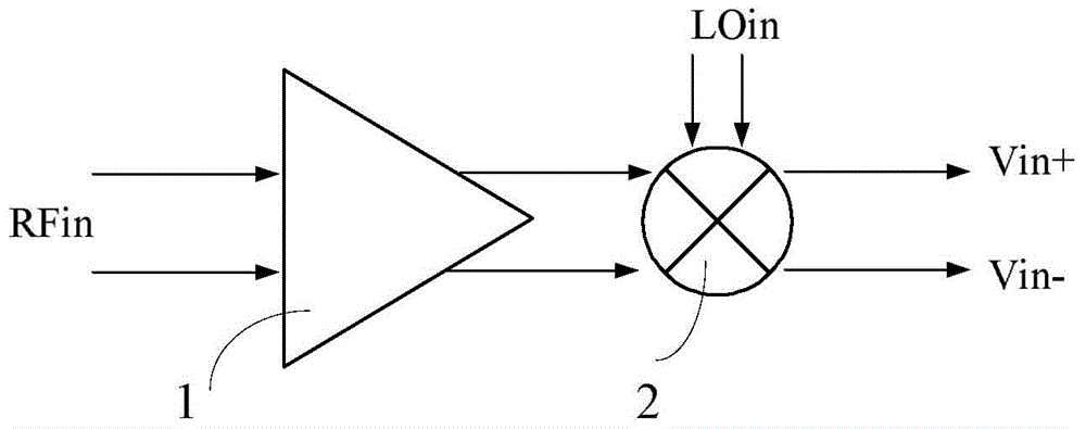
[0023] see figure 1 , The CMOS RF receiving front-end chip includes a low noise amplifier 1 and a mixer 2 . After the differential radio frequency signal RFin is amplified by the low noise amplifier 1 , it is mixed with the local oscillator signal LOin by the mixer 2 to output a positive output signal Vin+ and a negative output signal Vin−.

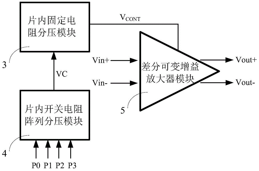
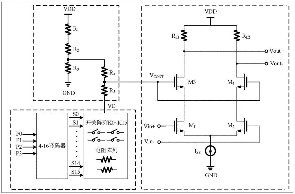
[0024] The circuit of the present invention is used to solve figure 1 The problem of inconsistency in gain between batches of CMOS RF receiving front-end chips. Please combine figure 2 , the circuit includes an on-chip fixed resistor voltage divider modul...


PUM


Abstract

The invention discloses a circuit for solving inconsistency of gains among batches of chips, which is used for solving the inconsistency of gains among batches of chips of a CMOS (Complementary Metal-Oxide-Semiconductor Transistor) radio frequency receiving front end. The circuit comprises an in-chip fixed resistance voltage-dividing module, an in-chip switch resistance voltage-dividing module, and a difference variable gain amplifier module with a gain changing along with the change of a control voltage index. An end point VC of the in-chip switch resistance voltage-dividing module controls voltage division through a plurality of control word ports to generate a VC voltage value, and the VC voltage value is combined with the in-chip fixed resistance voltage-dividing module to generate control voltage. A difference radio frequency signal is amplified by a low-noise amplifier, and is subjected to frequency mixing together with a local signal through a frequency mixer to output a positive output signal and a negative output signal. The in-phase end and the inverse-phase end of the difference variable gain amplifier module respectively receive the positive output signal and the negative output signal of the frequency mixer, the control end of the difference variable gain amplifier module receives control voltage, and the control voltage controls the difference variable gain amplifier module to output a plurality of gains to be selected.

Description

technical field [0001] The invention relates to a circuit for solving gain inconsistency between batches of chips, in particular to a circuit for solving gain inconsistency between batches of CMOS radio frequency receiving front-end chips. Background technique [0002] The RF receiving front-end is the core part of the RF receiver, and its gain stability has a great impact on the performance of the entire system such as gain and noise. However, the process flow of the process manufacturer is generally extremely complicated and requires precision, and any slight change in the process flow may cause serious problems. Gain inconsistency between chip batches often exists, but the change is different in size. In practice, a small chip gain inconsistency may not bring more problems to the system. However, the large chip gain inconsistency may affect the normal operation of the system. In severe cases, it will directly affect the application of the entire batch of chips, resulting ...

Claims


Application Information

Patent Timeline
Patent Type & Authority Applications(China)
IPC IPC(8): H03G3/20H03F1/26H03F3/45H04B1/16
Inventor 王晓东段宗明马强王曾祺李智群
Owner CHINA ELECTRONIC TECH GRP CORP NO 38 RES INST
Why Eureka
Try Eureka