Method of preparing a groove grid-control power device

A technology for power devices and trench gates, which is used in semiconductor devices, semiconductor/solid-state device manufacturing, electrical components, etc., and can solve problems such as poor terminal structure, complicated steps, and poor breakdown voltage and reliability of semiconductor devices.

Inactive Publication Date: 2014-03-12
SHENZHEN LIZHEN SEMICON
View PDF1 Cites 5 Cited by
  • Summary
  • Abstract
  • Description
  • Claims
  • Application Information

AI Technical Summary

Problems solved by technology

[0005] In the existing trench power MOSFET design and manufacturing field, the base region and the source region of the MOSFET are introduced by the steps of base region mask and source region mask respectively. In order to reduce the manufacturing cost, some previous proposals, Such as an article published in the Japanese Journal of Applied Physics (Japanese Journal of Applied Physics Vol 47, No.3, 2008,

Method used


Image

  • Method of preparing a groove grid-control power device
  • Method of preparing a groove grid-control power device
  • Method of preparing a groove grid-control power device

Examples


Embodiment 1

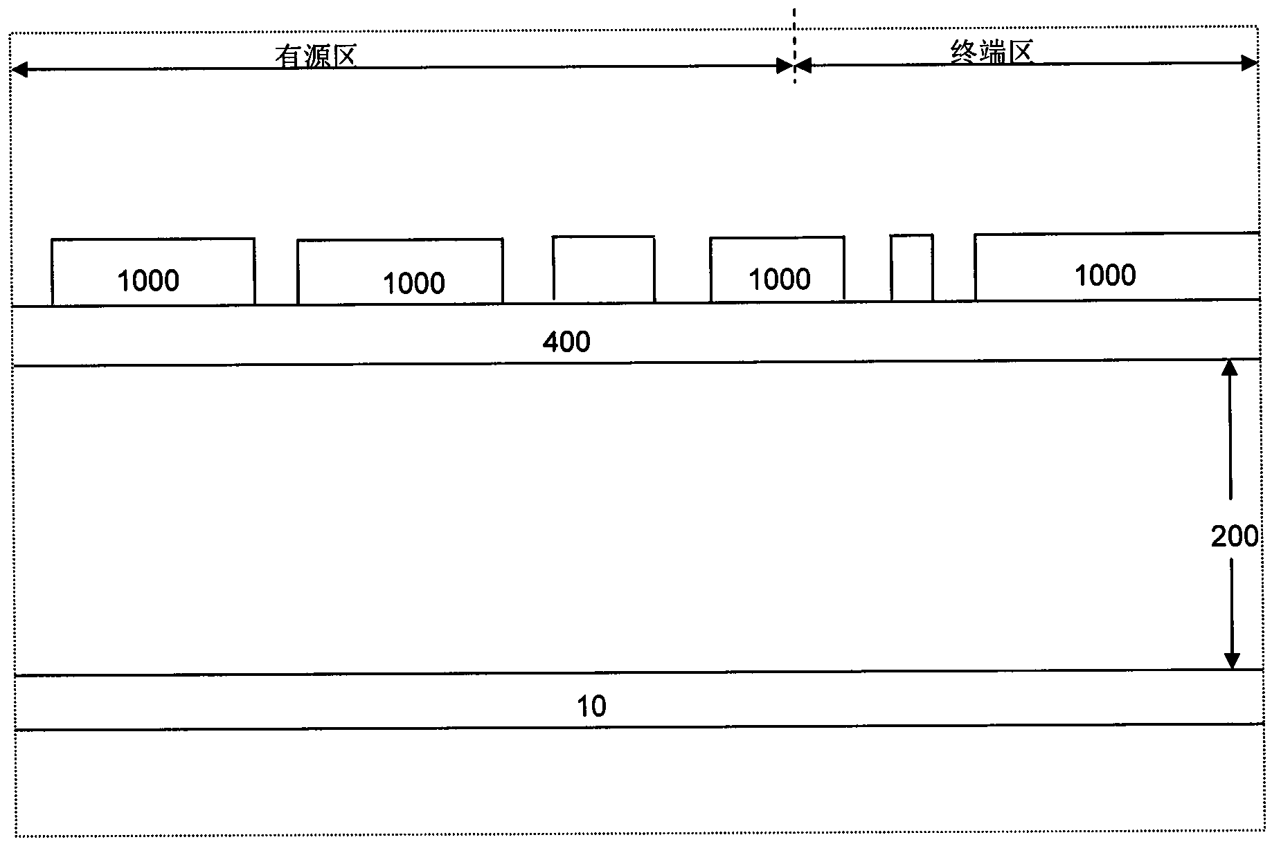
[0086] Such as figure 1 As shown, the epitaxial layer 200 is placed above the substrate 10. First, an oxide layer 400 (with a thickness of 0.3um to 1.5um oxide hard mask) is formed on the epitaxial layer by deposition or thermal growth, and then on the oxide layer A photoresist coating 1000 is deposited and then patterned through a trench mask to expose portions of the oxide layer.

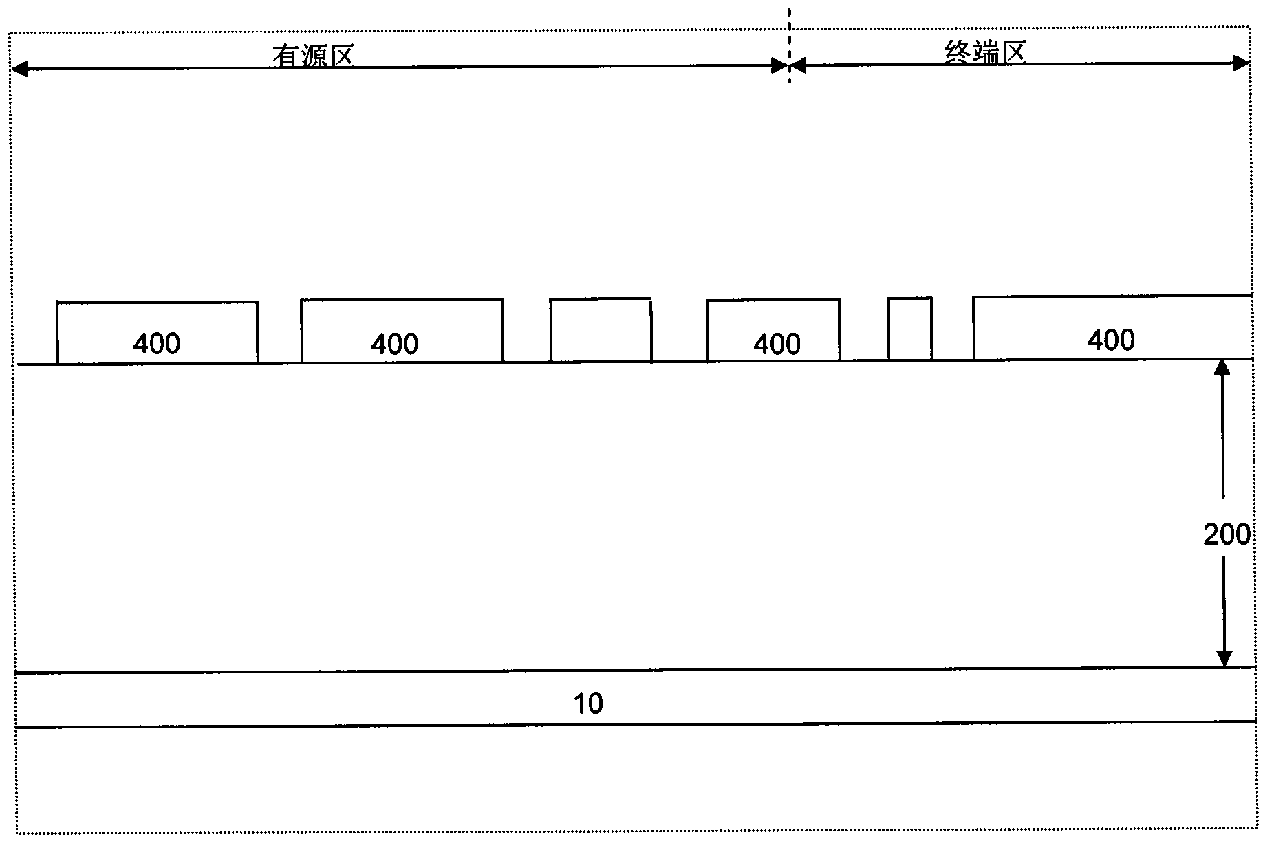
[0087] Such as figure 2 As shown, after dry etching the oxide layer exposed by patterning the trench mask, the epitaxial layer is exposed, and then the photolithographic coating is removed.

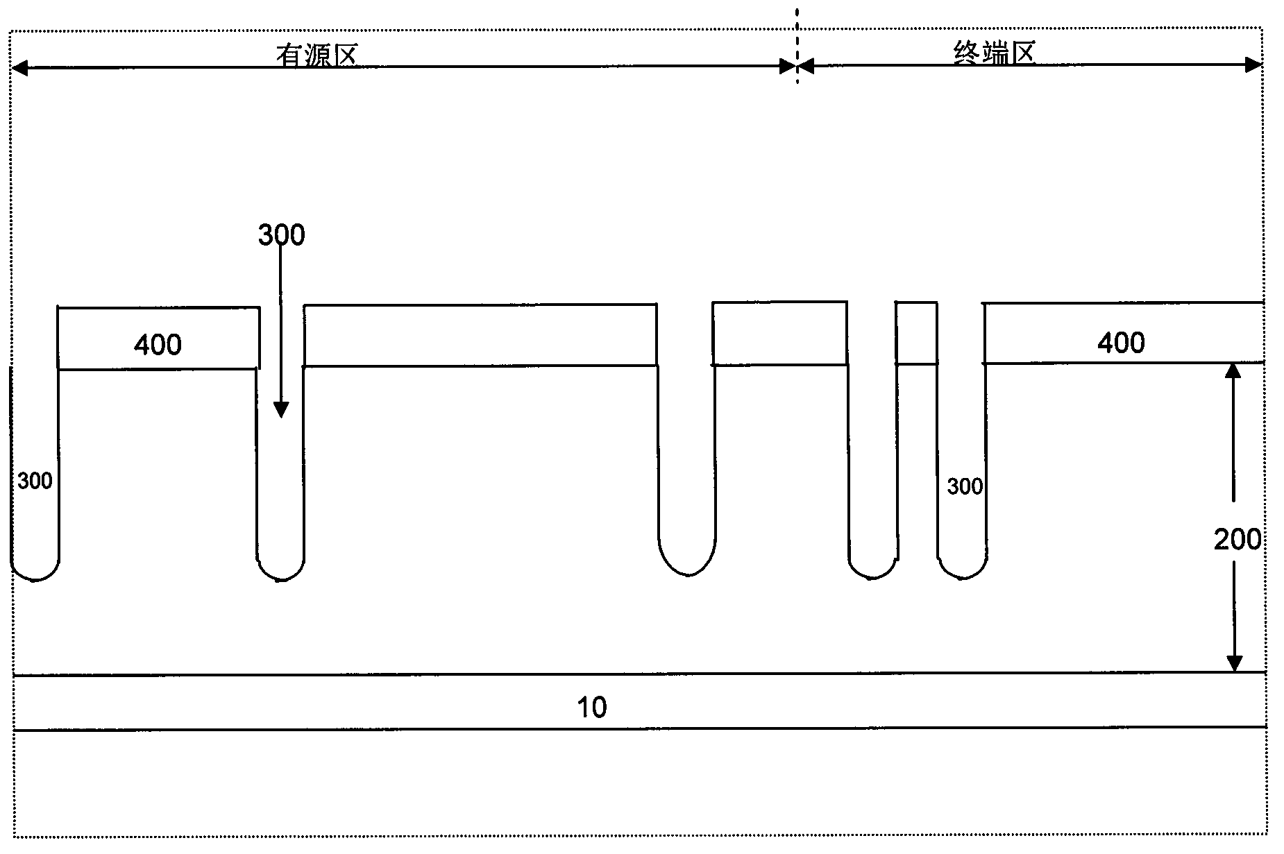
[0088] Such as image 3 As shown, a trench 300 is formed by etching, and the trench (0.8um to 5.0um in depth and 0.12um to 1.5um in width) extends to the N-type epitaxial layer.

[0089] Such as Figure 4 As shown, after the trench is formed, the trench is sacrificially oxidized (10 minutes to 100 minutes at a temperature of 1000°C to 1200°C) to eliminate the silicon layer damaged by the plasma during t...

Embodiment 2

[0100] It is an embodiment of the present invention.

[0101] Step and embodiment 1 are by Figure 1 to Figure 8 Same, then utilize the source region mask step to form the N-type source region 204, and the remaining steps are the same as in Embodiment 1 by Figure 10 to Figure 13 same.


PUM

PropertyMeasurementUnit
Thicknessaaaaaaaaaa
Thicknessaaaaaaaaaa
Thicknessaaaaaaaaaa

Abstract

The invention discloses a method of preparing a groove grid-control power device, the method comprising the steps of first eroding an epitaxial layer on a substrate by use of a groove mask to form a plurality of grooves; then, injecting a P-type dopant and an N-type dopant into the epitaxial layer to form a P-type base region and an N-type source region respectively, then depositing an interlayer dielectric on the surface of the epitaxial layer, eroding the interlayer dielectric by use of a contact hole mask to form an opening in the interlayer dielectric, eroding the surface of the epitaxial layer later to form a contact hole groove and carrying out metal plugging filling on the contact hole groove; and finally, depositing a metal layer on the surface of a device, and carrying out metal eroding by use of a metal mask to form a metal cushion layer and connection wires. By adopting the method of preparing the groove grid-control power device, preparation procedures of base region masking and source region masking are eliminated, and the preparation cost of the device is greatly reduced.

Description

technical field [0001] The invention relates to the technical field of semiconductor power discrete devices, in particular to a preparation method of a trench-type semiconductor power discrete device. Background technique [0002] At present, power MOSFET (Metal Oxide Semiconductor Field Effect Transistor, Metal Oxide Semiconductor Field Effect Transistor) has been widely used in various electronic and communication products, computers, consumer appliances, automobiles, etc. At the same time, it also has various applications in industry. [0003] Power semiconductor devices represented by power MOSFETs can effectively control high-frequency large currents due to their low on-resistance and high-speed switching. At the same time, power MOSFETs are being widely used as small power conversion components such as power amplifiers, power converters, low noise amplifiers, and some personal computer power supply switches and power circuits, which are characterized by low power consu...

Claims


Application Information

Patent Timeline
IPC IPC(8): H01L21/336
CPCH01L29/66613
Inventor 苏冠创
Owner SHENZHEN LIZHEN SEMICON
Why Eureka
Try Eureka