SMD laser packaging structure and packaging method in optoelectronic circuit

A packaging structure and laser technology, applied in lasers, laser parts, semiconductor lasers, etc., to achieve the effects of reducing packaging costs, avoiding damage rates, and excellent insulation performance

Active Publication Date: 2016-08-03
Shandong Huaguang Optoelectronics Co. Ltd.
View PDF5 Cites 1 Cited by
  • Summary
  • Abstract
  • Description
  • Claims
  • Application Information

AI Technical Summary

Problems solved by technology

However, low-cost, large-scale use of SMD packaged semiconductor lasers has rarely been reported.

Method used


Image

  • SMD laser packaging structure and packaging method in optoelectronic circuit
  • SMD laser packaging structure and packaging method in optoelectronic circuit

Examples


Embodiment 1

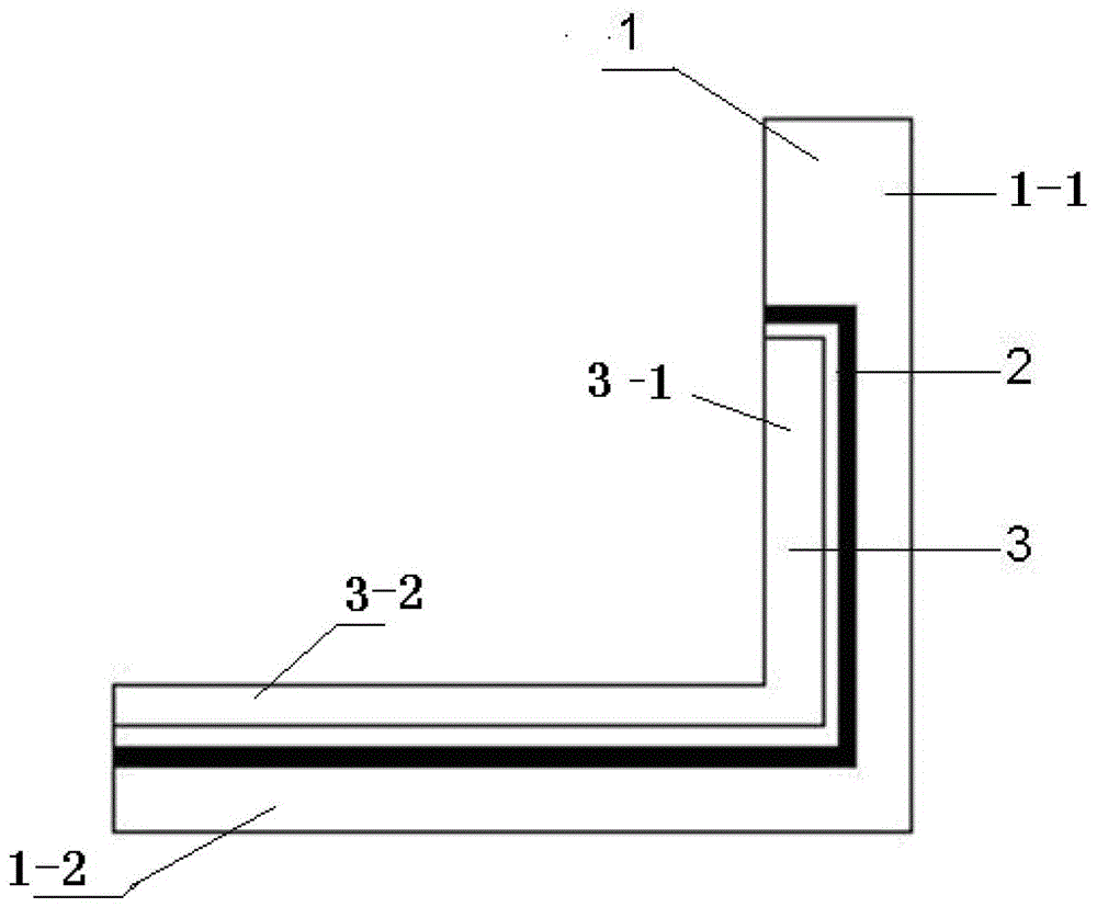
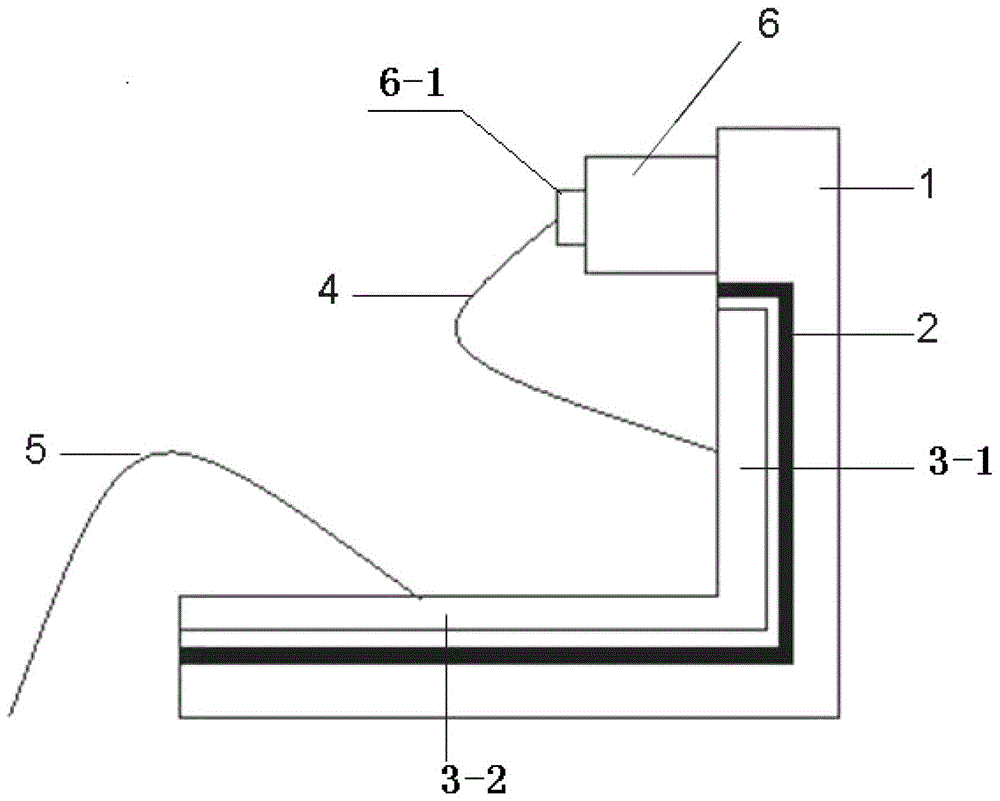
[0035] A chip-type laser packaging structure, including a semiconductor laser tube core 6 and an L-shaped heat sink; the L-shaped heat sink includes an L-shaped negative electrode layer 1, an L-shaped insulating layer 2, and an L-shaped positive electrode layer 3, An L-shaped groove is provided on the inner surface of the L-shaped negative electrode layer 1, and the L-shaped positive electrode layer 3 is embedded in the L-shaped groove, and the L-shaped negative electrode layer 1 and An L-shaped insulating layer 2 is arranged between the L-shaped anode layers 3 ; the semiconductor laser die 6 is mounted on the inner surface of the L-shaped anode layer 1 without L-shaped grooves.

[0036] The material of the L-shaped negative electrode layer is copper.

[0037] The material of the L-shaped positive electrode layer is copper.

[0038] The material of the L-shaped insulating layer is glass fiber.

Embodiment 2

[0040] A chip-type laser packaging structure as described in Embodiment 1, the difference is that the material of the L-shaped negative electrode layer 1 is single crystal silicon. The material of the L-shaped anode layer 3 is single crystal silicon.

[0041] The material of the L-shaped insulating layer 2 is silicone grease. The silicone grease described is DX-9041 thermal conductive silicone grease, commonly known as heat dissipation paste, which has good thermal conductivity, temperature resistance, and insulation properties. It is an ideal dielectric material for heat-resistant devices, and its performance is stable, and it will not produce Corrosive gases that do not affect the metals they come in contact with.

Embodiment 3

[0043] A patch laser package structure as described in Example 1, the difference is that the material of the L-shaped insulating layer is an insulating heat-conducting adhesive, and the insulating heat-conducting adhesive is a type of one-component room temperature vulcanized silicone Adhesive has the characteristics of convenient use, high bonding strength, elastic body after curing, impact resistance, vibration and so on. At the same time, the cured product also has good heat conduction, heat dissipation function, excellent high and low temperature resistance and electrical performance.


PUM


Abstract

The invention discloses a surface-mounted type laser packaging structure comprising a semiconductor laser tube core and an L-shaped heat sink. The L-shaped heat sink comprises an L-shaped negative electrode layer, an L-shaped insulating layer and an L-shaped positive electrode layer. An L-shaped groove is arranged on the internal surface of the L-shaped negative electrode layer The L-shaped positive electrode layer is arranged in the L-shaped groove in an embedded way. The L-shaped insulating layer is arranged between the L-shaped negative electrode layer and the L-shaped positive electrode layer. The semiconductor laser tube core is installed on the part, which has no L-shaped groove, of the internal surface of the L-shaped negative electrode layer. The surface-mounted type laser packaging structure is small in volume, high in reliability and low in welding point defect rate. Besides, automation is easy to realize, production efficiency is enhanced and cost is lowered.

Description

technical field [0001] The invention relates to a chip-type laser package structure and a package method thereof in a photoelectric circuit, belonging to the technical field of semiconductor laser packages. Background technique [0002] In recent years, high-power lasers have been increasingly produced for many applications, such as direct material processing, fiber laser and amplifier pumping, free-space optical communications, printing and medical treatment. These are mainly attributed to the development of laser structure design, semiconductor materials and reliable packaging technology. In particular, the packaging of the semiconductor laser enables the laser device to obtain high wall plugging efficiency, improve stability and save the user's use cost. The packaging structure of semiconductor lasers is roughly divided into two types according to the power of semiconductor lasers: semiconductor lasers with output power of 1W or 1W mostly use TO packaging structure, whic...

Claims


Application Information

Patent Timeline
Patent Type & Authority Patents(China)
IPC IPC(8): H01S5/022H01S5/024
Inventor 夏伟张秋霞左致远陈康
Owner Shandong Huaguang Optoelectronics Co. Ltd.
Why Eureka
Try Eureka