Metal-silicon dioxide multilayer film hollow nano structure array and preparation method thereof
A silicon dioxide and hollow nanotechnology, which is applied in the fields of nanostructure manufacturing, nanotechnology, nanotechnology, etc., can solve the problems of low manufacturing efficiency, difficulty in realizing controllable preparation of metal-silica thin film hollow nanostructure arrays, and high cost , to achieve the effect of large interior space
- Summary
- Abstract
- Description
- Claims
- Application Information
AI Technical Summary
Problems solved by technology
Method used
Image

Examples
Embodiment 1
[0044] Embodiment 1: Gold-chromium-silicon dioxide three-layer film nano-pyramid structure array and its preparation method
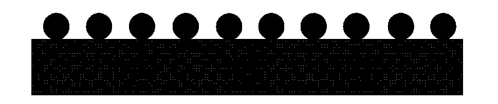
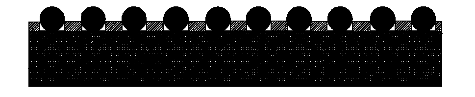
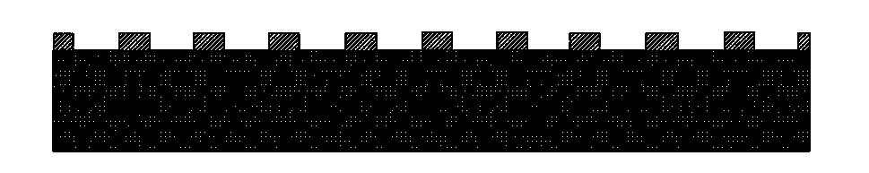
[0045] A metal-silicon dioxide multilayer film hollow nanostructure array of the present invention is specifically a gold-chromium-silicon dioxide three-layer film nano-pyramid structure array, such as Figure 11 As shown, it includes a glass substrate 1, and the surface of the glass substrate 1 is sequentially provided with a silicon dioxide film nano-pyramid structure array 2 (that is, a silicon dioxide film hollow nano-structure array), a chromium film nano-structure array 3 and a gold film Nanostructure arrays4. The gold-chromium-silicon dioxide three-layer thin film nano-pyramid structure array is a two-dimensional periodically arranged hexagonal array structure, that is, the silicon dioxide film nano-pyramid structure array 2, the chromium film nano-structure array 3 and the gold film nano-structure array 4 are all It is a two-dimensional perio...
Embodiment 2
[0066] Example 2: Gold-silver-silicon dioxide three-layer thin film nano-cylinder structure array and its preparation method
[0067] A metal-silicon dioxide multilayer thin film hollow nanostructure array of the present invention is specifically a gold-silver-silicon dioxide three-layer thin film nano cylinder structure array, such as Figure 13 As shown, a glass substrate 1 is included, and a silicon dioxide film nano-cylinder structure array 5, a silver film nano-structure array 6 and a gold film nano-structure array 4 are sequentially arranged on the surface of the glass substrate 1 from bottom to top. The gold-silver-silica three-layer thin-film nano-cylindrical structure array is a two-dimensional periodic array structure of hexagonal arrays, that is, the silicon dioxide thin-film nano-cylindrical structure array 5, the silver film nano-structure array 6 and the gold film nano-structure array 4 are two-dimensional periodic arrangement of the hexagonal array structure. ...
Embodiment 3
[0085] Example 3: Aluminum-chromium-silicon dioxide three-layer thin film nanocap structure array and its preparation method
[0086] A metal-silicon dioxide multilayer thin film hollow nanostructure array of the present invention is specifically a gold-silver-silicon dioxide three-layer thin film nanocap structure array, such as Figure 15 As shown, a glass substrate 1 is included, and a silicon dioxide film nanocap structure array 7, a chromium film nanostructure array 3 and an aluminum film nanostructure array 8 are sequentially arranged on the surface of the glass substrate 1 from bottom to top. The gold-silver-silica three-layer thin film nanocap structure array is a two-dimensional periodic array structure of hexagonal arrays, that is, the silicon dioxide thin film nanocap structure array 7, the chromium film nanostructure array 3 and the aluminum film nanostructure array 8 are all It is a two-dimensional periodic hexagonal array structure. The maximum diameter of the...
PUM
| Property | Measurement | Unit |
|---|---|---|
| thickness | aaaaa | aaaaa |
| thickness | aaaaa | aaaaa |
| thickness | aaaaa | aaaaa |
Abstract
Description
Claims
Application Information