Method for preparing non-polar zinc oxide thin film on silicon-based substrate

A non-polar, thin-film technology, applied in the field of functional material preparation, can solve the problems of increased energy consumption, high turn-on voltage, unfavorable electrical conductivity, etc., and achieve the effect of smooth surface

Inactive Publication Date: 2014-03-19
NORTH CHINA UNIVERSITY OF TECHNOLOGY
View PDF2 Cites 3 Cited by
  • Summary
  • Abstract
  • Description
  • Claims
  • Application Information

AI Technical Summary

Problems solved by technology

[0004] In summary, the existing substrates for the preparation of (110) oriented non-polar ZnO films are oxide single crystal materials, such as SrTiO 3 (STO), LaAlO 3 and Al 2 o 3 Such bulk single crystal substrates are expensive and small in area, and non-polar ZnO thin films prepared on oxide single crystal substrates cannot be integrated with Si-based substrates on a large scale
At the same time, most of the buffer layers used in the preparation of Si-based non-polar ZnO thin films are insulating materials, such as Al 2 o 3 , which is not conducive to the conductive properties between non-polar ZnO thin films and other thin films (such as for PN junction devices such as electroluminescence and photodetection), which will lead to problems such as high turn-on voltage and increased energy consumption.

Method used


Image

  • Method for preparing non-polar zinc oxide thin film on silicon-based substrate
  • Method for preparing non-polar zinc oxide thin film on silicon-based substrate
  • Method for preparing non-polar zinc oxide thin film on silicon-based substrate

Examples


Embodiment 1

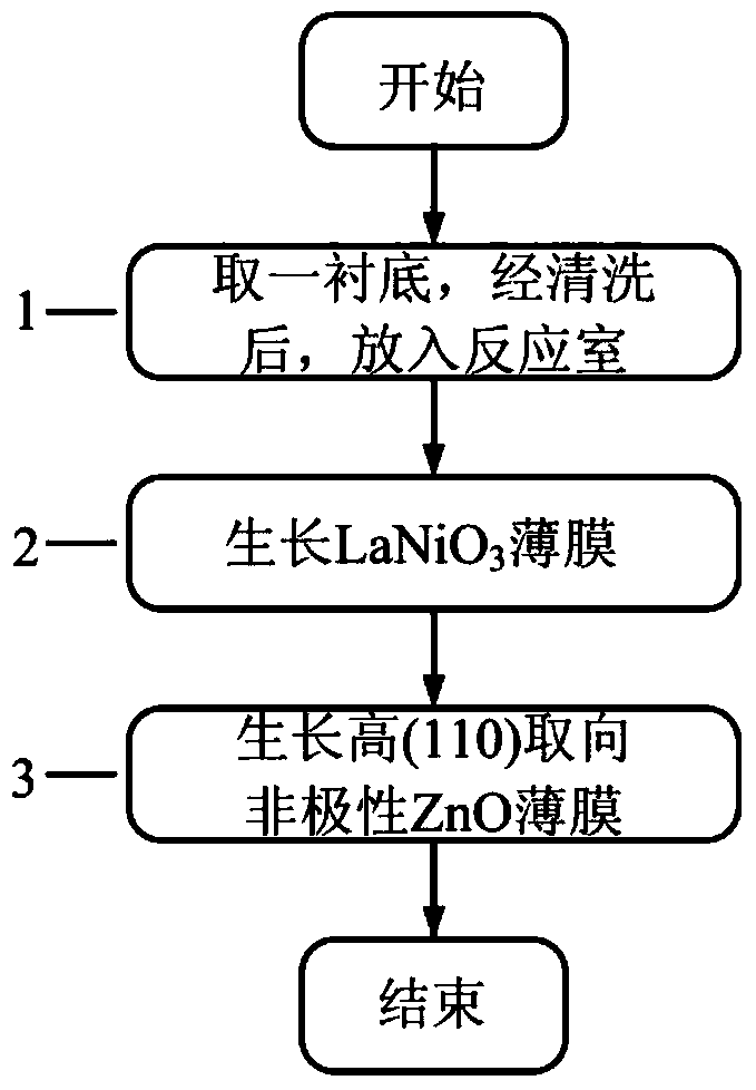
[0035] (1) Take one (100) crystal-oriented single-crystal Si wafer substrate, use ultrasonic cleaning, wash in acetone, ethanol and deionized water for 10 minutes, and then dry it with nitrogen gas for later use;

[0036] (2) Before the experiment starts, the vacuum degree of the reaction chamber is controlled to be 8×10 -4 Below Pa, the speed of the sputtering table is maintained at 15rad / s; first, the (100) Si substrate is heated to 300°C, and the purity is 99.99% LaNiO 3 Ceramic target pre-sputtering 30min, working gas Ar and O 2 The flow ratio is 1:4, the sputtering power and working pressure are controlled to be 250W and 0.5Pa, respectively, after sputtering for 60min, take it out, and anneal at 700°C for 30min to obtain LaNiO with a layer thickness of 90nm. 3 Conductive film;

[0037] (3) Before the experiment starts, the vacuum degree of the reaction chamber is controlled to be 8×10 -4 Below Pa, the speed of the sputtering table is maintained at 15rad / s; the (100) or...


PUM

PropertyMeasurementUnit
thicknessaaaaaaaaaa
thicknessaaaaaaaaaa
thicknessaaaaaaaaaa

Abstract

The invention provides a method for preparing a high (110) oriented non-polar zinc oxide thin film on a Si-based substrate. The method comprises the steps of taking Si as a substrate, taking a ZnO target material as a zinc source and an oxygen source, taking Ar as working gas, taking O2 as reaction gas, adopting a magnetron sputtering method, controlling the vacuum degree below 8*10<-4>Pa, controlling the growth temperature at 100-400 DEG C and simultaneously introducing Ar and O2 in a certain proportion to prepare the thin film. The method comprises the steps of growing a (100) oriented LaNiO3 (LNO) buffer layer on the Si-based substrate and growing a high (110) oriented ZnO thin film on a (100) LNO / Si substrate. By adding the LNO buffer layer, the growth of the high (110) oriented non-polar ZnO thin film can be effectively realized, the band-edge emission in a photoluminescence spectrum is obviously enhanced, and a defect luminescence peak is obviously weakened.

Description

technical field [0001] The invention relates to semiconductor thin film materials, in particular to wide bandgap semiconductor materials, and belongs to the technical field of functional material preparation. Background technique [0002] Due to the wide bandgap (3.36eV) and large exciton binding energy (60meV), ZnO material is easy to obtain strong exciton emission at room temperature, and can become an important material for ultraviolet lasers, especially in ultraviolet light-emitting diodes, lasers and detectors. It has important research and application value. [0003] ZnO thin films can be divided into polar and non-polar thin films. In the prior art, the substrates for preparing non-polar ZnO thin films mainly use SrTiO 3 (STO), LaAlO 3 and Al 2 o 3 and other bulk single crystal substrates. For example, Wu et al. of Tsinghua University (Wu et al., Structural and electrical properties of (110) ZnO epitaxial thin films on (001) SrTiO 3 substrates.Solid State Commu...

Claims


Application Information

Patent Timeline
Patent Type & Authority Applications(China)
IPC IPC(8): C23C14/35C23C14/08C23C14/58
Inventor 赵全亮何广平狄杰建袁俊杰王大伟苏德志李中翔
Owner NORTH CHINA UNIVERSITY OF TECHNOLOGY
Why Eureka
Try Eureka