Pattern-segmented sapphire substrate used for AlGaInN material system film growth

A sapphire substrate and thin film growth technology, which is applied in semiconductor devices, stone processing equipment, fine working devices, etc.

Inactive Publication Date: 2014-03-19
NANCHANG UNIV +1
View PDF7 Cites 2 Cited by
  • Summary
  • Abstract
  • Description
  • Claims
  • Application Information

AI Technical Summary

Problems solved by technology

However, the current laser lift-off technology is still immature, and the yield rate of chip manufacturing is low, which also hinders the development of vertical structure LEDs on sapphire substrates to a certain extent.

Method used


Image

  • Pattern-segmented sapphire substrate used for AlGaInN material system film growth
  • Pattern-segmented sapphire substrate used for AlGaInN material system film growth
  • Pattern-segmented sapphire substrate used for AlGaInN material system film growth

Examples


Embodiment 1

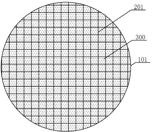
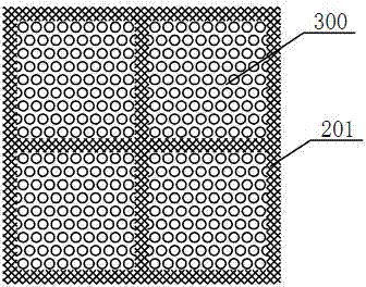
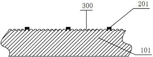
[0040] Such as Figure 1 to Figure 4 As shown, a split pattern sapphire substrate for AlGaInN material system film growth includes: a sapphire substrate body 100, a pattern split groove 200 is processed on the upper surface of the sapphire substrate body 100, and the pattern split groove 200 will The upper surface of the sapphire substrate body 100 is divided into a plurality of independent and non-connected repeated pattern units 300 , and the AlGaInN thin film 400 is grown on the pattern units 300 .

[0041] In this embodiment, the sapphire substrate body 100 adopts a patterned sapphire substrate body 101 , and the pattern dividing groove 200 adopts a second medium type pattern dividing groove 201 .

[0042] Wherein: the second dielectric pattern dividing groove 201 can be obtained by first depositing a dielectric film on the sapphire substrate, and then using photolithography technology, the width of the second dielectric pattern dividing groove 201 is 10 microns, and the h...

Embodiment 2

[0047] The structure of embodiment 2 is basically the same as embodiment 1, the difference is: as Figure 5 to Figure 8 As shown, the sapphire substrate body 100 adopts a planar sapphire substrate body 102 .

[0048] The width of the second dielectric pattern dividing groove 201 is 20 microns, and the height is 0.1 microns.

[0049] The graphics unit 300 is a rectangle with a size of 2mm×3mm.

Embodiment 3

[0051] The structure of embodiment 3 is basically the same as embodiment 1, the difference is: as Figure 9 to Figure 12 As shown, the sapphire substrate body 100 adopts a planar sapphire substrate body 102 , and the pattern dividing groove 200 adopts a groove type pattern dividing groove 202 .

[0052] The trench-type pattern dividing groove 202 can be obtained by dry or wet etching of the sapphire substrate using photolithography technology. The width of the groove-type pattern dividing groove 202 is 20 microns, and the depth is 20 microns.

[0053] The graphics unit 300 is a square with a size of 2mm×2mm.


PUM

PropertyMeasurementUnit
lengthaaaaaaaaaa
widthaaaaaaaaaa
heightaaaaaaaaaa

Abstract

The invention discloses a pattern-segmented sapphire substrate used for AlGaInN material system film growth. The pattern-segmented sapphire substrate comprises a sapphire substrate body; pattern segmentation grooves divide the upper surface of the sapphire substrate body into a plurality of mutually-independent repeated pattern units, wherein the pattern units are growing platforms of AlGaInN materials. The sapphire substrate body is a plane sapphire substrate body or a pattern sapphire substrate body. The pattern segmentation grooves are trench-type pattern segmentation grooves or second medium-type pattern segmentation grooves. The pattern-segmented sapphire substrate is formed by dividing the sapphire substrate into the plurality of mutually-independent and mutually-isolated pattern units through the grooves or second medium. According to the segmented AlGaInN epitaxial thin films, the wave length uniformity of an LED can be greatly improved, the qualified rate of an LED epitaxial wafer is improved, and the giant thermal stress and thermal shock, due to laser lift-off, between the AlGaInN epitaxial thin films and the sapphire substrate are greatly reduced, the pass rate of the laser lift-off can be greatly improved, and the qualified rate of sapphire substrate vertical structure LED chips is improved.

Description

technical field [0001] The invention belongs to the AlGaInN material system thin film growth technology, in particular to a split pattern sapphire substrate used for AlGaInN material system thin film growth. Background technique [0002] In recent years, with the continuous progress of AlGaInN material system LED technology, LED has been gradually used in display, backlight, lighting and other fields. After the luminous efficiency has completely surpassed traditional lamps such as incandescent lamps and fluorescent lamps, the biggest problem preventing LED lighting from fully entering general lighting is how to further reduce costs. At present, the main ways to reduce the cost are to increase the size of the epitaxial substrate or to improve the luminous efficiency of LED under high current density. Among them: increasing the size of the epitaxial substrate can significantly increase the number of chips produced by a single epitaxial wafer, thereby reducing the cost of the ...

Claims


Application Information

Patent Timeline
Patent Type & Authority Applications(China)
IPC IPC(8): H01L33/00H01L33/22B28D5/00B23K26/36
CPCH01L21/02005B28D5/0005H01L33/0066H01L33/20
Inventor 刘军林江风益
Owner NANCHANG UNIV
Why Eureka
Try Eureka