
Method for preparing germanium oxide interface repairing layer by using in-situ ozone oxidation

A technology of ozone oxidation and germanium oxide, which is applied in the manufacture of semiconductor/solid-state devices, semiconductor devices, electrical components, etc., can solve the problems of harsh conditions and high consumption costs, and achieve the effects of convenient control, reduction of other pollution, and low cost

Inactive Publication Date: 2014-03-26
INST OF MICROELECTRONICS CHINESE ACAD OF SCI
View PDF7 Cites 1 Cited by
  • Summary
  • Abstract
  • Description
  • Claims
  • Application Information

AI Technical Summary

Problems solved by technology

Other existing methods for preparing the germanium oxide interface layer require relatively harsh conditions and relatively high consumption costs

Method used


Image

  • Method for preparing germanium oxide interface repairing layer by using in-situ ozone oxidation
  • Method for preparing germanium oxide interface repairing layer by using in-situ ozone oxidation
  • Method for preparing germanium oxide interface repairing layer by using in-situ ozone oxidation

Examples


Embodiment Construction

[0024] In order to make the object, technical solution and advantages of the present invention clearer, the present invention will be described in further detail below in conjunction with specific embodiments and with reference to the accompanying drawings.

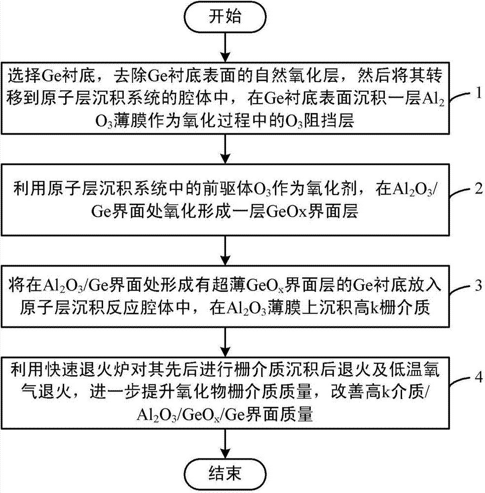
[0025] The invention provides a method for preparing a germanium oxide interface repair layer on a Ge substrate by in-situ ozone oxidation, repairing the high-k gate dielectric / Ge interface, so as to realize the interface stability and stability required by the gate stack in Ge-based MOS devices. high quality. This method includes the following steps: first remove the natural oxide layer on the surface of the Ge substrate, and quickly transfer it to the cavity of the atomic layer deposition system to deposit a thin layer of Al 2 o 3 thin film; then using the precursor O in the atomic layer deposition system 3 As an oxidizing agent, in Al 2 o 3 / Ge interface is oxidized to form a layer of GeO x The interface layer; th...


PUM

PropertyMeasurementUnit
thicknessaaaaaaaaaa

Abstract

The invention discloses a method for preparing a germanium oxide interface repairing layer by using in-situ ozone oxidation. The method comprises the steps of: selecting a Ge substrate, removing a natural oxide layer on the surface of the Ge substrate, then transferring the Ge substrate in a cavity of an atomic layer deposition system, and depositing a layer of Al2O3 film on the surface of the Ge substrate to serve as an O3 barrier layer in an oxidation process; oxidizing at an Al2O3 / Ge interface to form a layer of a GeOx interface layer by using a precursor O3 in the atomic layer deposition system as an oxidant; placing the Ge substrate with the ultra-thin GeOx interface layer formed at the Al2O3 / Ge interface into the atomic layer deposition reaction cavity, and depositing a high-k gate medium on the Al2O3 film; after gate medium deposition is carried out successively, performing annealing and low-temperature oxygen annealing by utilizing a rapid annealing furnace to further improve the quality of the oxide gate medium and improve the quality of the high-k medium / Al2O3 / GeOx / Ge interface. The method for preparing the germanium oxide interface repairing layer by using the in-situ ozone oxidation realizes interface stability and high quality required by a gate laminate layer in a Ge-based MOS (Metal Oxide Semiconductor) device, and is suitable for a Ge-based MOS capacitor, an MOSFET (MOSFET (Metal-Oxide-Semiconductor Field Effect Transistor) and other devices including the Ge-based gate laminate layer.

Description

technical field [0001] The invention relates to the field of semiconductor technology, in particular to a method for preparing ultra-thin germanium oxide (GeO) on a Ge substrate by in-situ ozone oxidation. x ) interface repair layer method. Background technique [0002] Germanium (Ge) has been extensively studied as the most promising substrate material for metal-oxide-semiconductor transistors (MOSFETs) in recent years. Compared with silicon, germanium has a high carrier mobility, and its drive current is small, which is suitable for low-temperature processes. In order to realize high-performance small-sized Ge-based MOSFETs, high-k gate stacks must have low interface state density and effectively passivated interface layers. The interface of high-k gate dielectric / Ge needs a special interface layer as a diffusion barrier layer to prevent the interface reaction between high-k metal oxide and Ge substrate under heat treatment conditions. The reported methods of interface ...

Claims


Application Information

Patent Timeline
Patent Type & Authority Applications(China)
IPC IPC(8): H01L21/28H01L21/285
CPCH01L21/28158H01L21/28211
Inventor 刘洪刚韩乐王盛凯孙兵常虎东赵威
Owner INST OF MICROELECTRONICS CHINESE ACAD OF SCI
Learn More