
Lateral bipolar transistor with composite structure

A technology of bipolar transistors and composite structures, which is applied in the direction of semiconductor devices, electrical components, circuits, etc., can solve the problems that the reverse conduction voltage ratio cannot be improved at the same time, and achieve compact structure, enhanced depletion, and improved resistance The effect of breaking voltage level

Active Publication Date: 2014-03-26
SUZHOU YINGNENG ELECTRONICS TECH
View PDF6 Cites 5 Cited by
  • Summary
  • Abstract
  • Description
  • Claims
  • Application Information

AI Technical Summary

Problems solved by technology

[0005] The technical problem to be solved by the present invention is that the dopant dose in the drift region of the lateral bipolar transistor with the SINGLE RESURF structure in the prior art has an opposite effect on the reverse blocking voltage and the specific on-resistance. The technical problem of on-voltage while reducing the specific on-resistance, providing a lateral bipolar transistor with a composite structure

Method used


Image

  • Lateral bipolar transistor with composite structure

Examples


Embodiment Construction

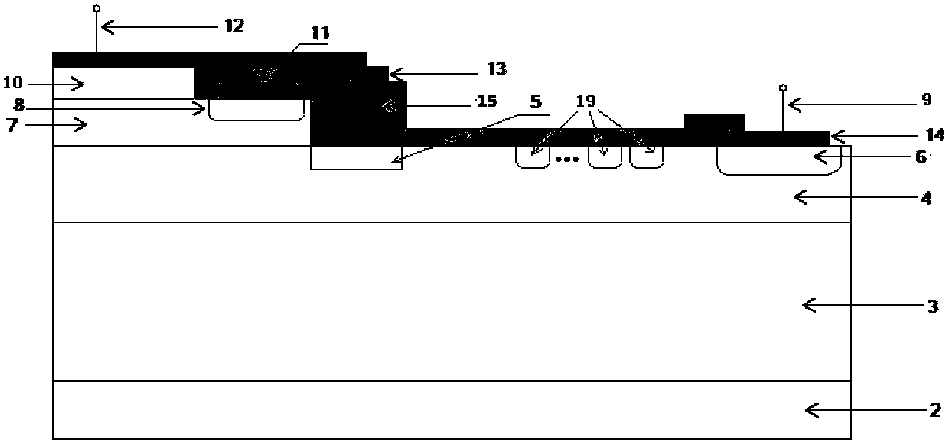
[0039] see figure 1 As shown, the lateral bipolar transistor with composite structure as Embodiment 1 of the present invention includes:

[0040] Included from bottom to top:

[0041] P + SiC substrate 2;

[0042] P - A silicon carbide epitaxial layer, the P silicon carbide epitaxial layer constitutes a P-type first RESURF region 3;

[0043] in the P - An N-type collector region 4 is formed on the silicon carbide by epitaxy, and a N-type collector region 4 is formed by ion implantation near the upper surface of the N-type collector region 4. +Collector area ohmic contact area 6, floating ring Floating Rings 19 and injected second RESURF area 5, wherein a collector electrode 9 is arranged on the N+ collector area ohmic contact area 6; the injected second RESURF area 5 It is used to gently change the electric field in the drift region. As a specific embodiment of the present invention, the second RESURF region 5 is a P-type RESURF region, and the length of the second RESUR...


PUM


Abstract

The invention relates to a lateral bipolar transistor with a composite structure. The lateral bipolar transistor particularly comprises a substrate and a first RESURF zone arranged on the substrate, as well as a current collection zone, a base zone and an emission zone which are arranged in sequence, and further comprises a second RESURF zone used for smoothing the change of the electric field of a drift zone and a plurality of floating rings formed at the periphery of the ohmic contact zone of the current collection zone, wherein an emitting electrode is arranged on the emission zone; the floating rings are positioned on the surface of the current collection zone and close to the ohmic contact zone; through the arrangement of the second RESURF zone, the electric field of the drift zone of the lateral bipolar transistor becomes smooth, and the specific on resistance of the whole device is further reduced; space charges of the floating rings are connected into a whole with a space charge in the drift zone of the current collection zone, so that the space charge area of the drift zone is increased, gathering of the space field at the edge of the ohmic contact zone of the current collection zone is greatly reduced, and under the condition of the same length of the drift zone, higher blocking voltage can be born.

Description

technical field [0001] The invention relates to a power device, in particular to a lateral bipolar transistor with composite structure. Background technique [0002] Power semiconductor devices are also called electronic power devices. With the development of power integrated circuits, especially single-chip power integrated systems, power semiconductor devices are booming. The electrodes of the lateral power device are located on the surface of the chip, and it is easy to realize mutual integration with low-voltage signal circuits and other devices through internal connections. Therefore, lateral power devices are widely used in power integrated circuits. In power integrated circuits, lateral power devices often account for more than half of the entire chip area, and are the core and key of the entire power integrated circuit. Moreover, with the development of modern power integrated circuits, higher requirements are put forward for the performance of lateral power devices...

Claims


Application Information

Patent Timeline
IPC IPC(8): H01L29/735H01L29/06
CPCH01L29/0634H01L29/735
Inventor 崔京京张作钦
Owner SUZHOU YINGNENG ELECTRONICS TECH
Learn More