A kind of preparation method of n-type back junction solar cell
A solar cell, N-type technology, applied in the field of solar cells, can solve the problems of poor diffusivity, difficult to dope uniformly, difficult to control uniformity, etc.
- Summary
- Abstract
- Description
- Claims
- Application Information
AI Technical Summary
Problems solved by technology
Method used
Image
Examples
Embodiment 1
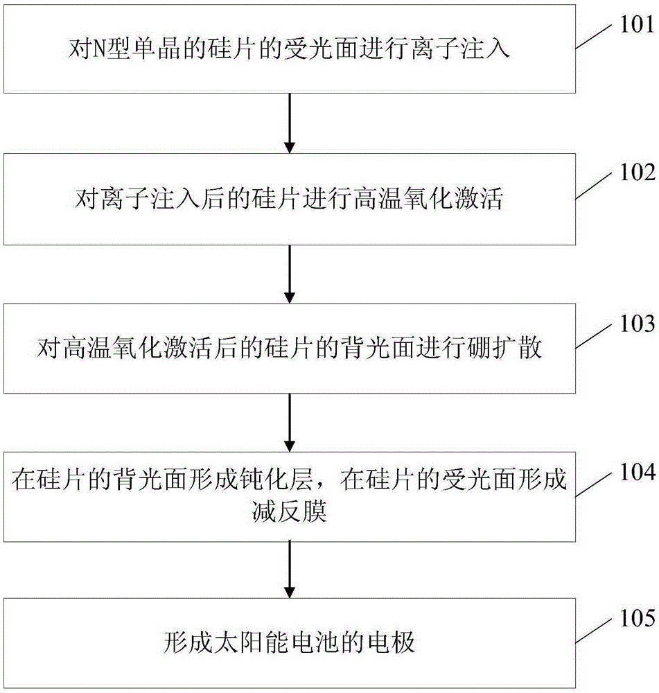
[0055] figure 1 It is an implementation flowchart of the manufacturing method of the N-type back-junction solar cell provided by the first embodiment of the present invention. Such as figure 1 As shown, the method provided by the embodiment of the present invention includes:
[0056] Step 101, performing ion implantation on the light-receiving surface of the N-type single crystal silicon wafer.
[0057] In the embodiment of the present invention, ion implantation is performed on the light-receiving surface of the silicon wafer, preferably, the implanted element is phosphorus. In the process of ion implantation, two kinds of doping concentrations that exist in intervals can be formed at one time by means of a "comb" type baffle, that is, two doping concentrations of small implantation amount and large implantation amount are formed respectively, which can reduce the size of the solar cell. The surface recombination of the light-receiving surface can also ensure high doping a...
Embodiment 2
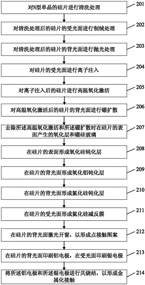
[0071] figure 2 It is an implementation flow chart of the manufacturing method of the N-type back junction solar cell provided by the second embodiment of the present invention. Such as figure 2 As shown, the method provided by the embodiment of the present invention includes:
[0072] Step 201 , cleaning the N-type single crystal silicon wafer.
[0073] Wherein, the chemical solution used for cleaning the silicon wafer is a silicon wafer cleaning agent (RCA) solution.
[0074] Specifically, an N-type monocrystalline silicon wafer with a thickness of 100 to 500 microns can be selected, and NH 4 OH (ammonium hydroxide): H 2 o 2 (hydrogen peroxide): H 2 O (water) = 1:1:6 RCA solution for cleaning to remove pollutants on the surface of the silicon wafer.
[0075] Step 202, performing texturing treatment on the light-receiving surface of the silicon wafer after cleaning.
[0076] Among them, the purpose of the texturing treatment is to corrode the relatively smooth surfa...
PUM
| Property | Measurement | Unit |
|---|---|---|
| thickness | aaaaa | aaaaa |
| thickness | aaaaa | aaaaa |
| thickness | aaaaa | aaaaa |
Abstract
Description
Claims
Application Information

