Method for reducing defects in silicon carbide epitaxial film

A technology of silicon carbide and silicon carbide on the silicon surface, which is applied in the direction of electrical components, semiconductor/solid-state device manufacturing, circuits, etc., can solve the problems of unfavorable device manufacturing, a large number of step-like morphology of epitaxial films, and unsatisfactory effect of eliminating defects. Achieve the effect of high epitaxial film quality, simple and easy method, and reduce defects

Active Publication Date: 2014-04-09
NO 55 INST CHINA ELECTRONIC SCI & TECHNOLOGYGROUP CO LTD
View PDF6 Cites 13 Cited by
  • Summary
  • Abstract
  • Description
  • Claims
  • Application Information

AI Technical Summary

Problems solved by technology

However, there are a large number of defects such as step-like morphology and triangular defects in the epitaxial film grown on the 4° off-angle substrate, which is not conducive to the later device fabrication
Although there have been some reports on reducing defects in epitaxial films on (0001) sili

Method used


Image

  • Method for reducing defects in silicon carbide epitaxial film
  • Method for reducing defects in silicon carbide epitaxial film
  • Method for reducing defects in silicon carbide epitaxial film

Examples


Embodiment 1

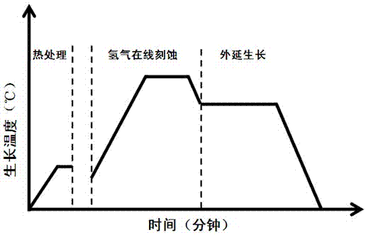
[0030] 1) Select the (0001) silicon surface 4H-SiC conductive substrate with a 4° bias to the direction and perform standard cleaning on it for use;

[0031] 2) Place the substrate on a hot graphite base, send it into the reaction chamber, and evacuate it to -6 mbar;

[0032] 3) After the prepared sample is sent to the reaction chamber and before the gas is introduced, the graphite reaction chamber (including the base) coated with tantalum carbide is heated by radio frequency induction, the radio frequency power is 5KW, the processing time is 15min, and the temperature is raised to 200°C;

[0033] 4) in H 2 The flow rate is 75L / min and the pressure of the reaction chamber is 100mbar. Slowly raise the temperature to 1570°C, keep the temperature constant for 10 minutes, and cool down to the epitaxial growth temperature of 1550°C in 10 minutes to remove surface damage and contamination, and at the same time help reduce Delay delay defects;

[0034] 5) The temperature is stabi...

Embodiment 2

[0037] 1) Select the (0001) silicon surface 4H-SiC high-purity semi-insulating substrate with a 4° bias to the direction and perform standard cleaning on it for use;

[0038] 2) Place the substrate on a hot graphite base, send it into the reaction chamber, and evacuate it to -6 mbar;

[0039] 3) After the prepared sample is sent to the reaction chamber and before the gas is introduced, the graphite reaction chamber (including the base) coated with tantalum carbide is heated by radio frequency induction, the radio frequency power is 6KW, the processing time is 20min, and the temperature is raised to 240°C;

[0040] 4) in H 2 The flow rate is 75L / min and the pressure of the reaction chamber is 100mbar. Slowly raise the temperature to 1590°C, keep the temperature constant for 5 minutes, and cool down to the epitaxial growth temperature of 1580°C in 10 minutes to remove surface damage and contamination, and at the same time help reduce Delay delay defects;

[0041] 5) The temp...


PUM


Abstract

The invention discloses a method for reducing defects in a silicon carbide epitaxial film. The method is executed in horizontal hot wall-type chemical vapor deposition (CVD) equipment and comprises the following steps of 1) substrate preparing, wherein a (0001) silicon-surface silicon carbide substrate deviating towards the (11-20) direction by 4 degrees is selected; 2) pre-growth baking, wherein a reaction chamber is subjected to radio frequency induction heating after a prepared sample is delivered to a reaction chamber and before gas is injected; 3) in-situ etching, wherein an improved hydrogen H2 in-situ etching technology is employed to perform pre-growth surface pre-treatment of the substrate; and 4) epitaxial growing, wherein a silicon carbide film starts to grow when the temperature rises to an epitaxial growth temperature. The advantages are that by using the method, the defects existing in the epitaxial film based on the (0001) silicon-surface silicon carbide substrate deviating towards the (11-20) direction by 4 degrees can be effectively reduced and the quality of the epitaxial film can be increased. The characteristics are that the method of the invention is simple and easy to implement; the epitaxial technology repeatability and consistency are good; the epitaxial film quality is high; and the method is suitable for mass production.

Description

technical field [0001] The present invention relates to a method for reducing defects in a homoepitaxial thin film based on a (0001) silicon surface silicon carbide substrate with a 4° bias to the <11-20> direction. It belongs to the technical field of semiconductor materials. Background technique [0002] In recent years, silicon carbide (SiC) epitaxial materials and devices are growing steadily and rapidly, and in some fields it is gradually replacing traditional silicon and gallium arsenide materials. Silicon carbide has better material properties than silicon and gallium arsenide. For example 4H-SiC, which has approximately 4×10 6 V / cm breakdown field strength, about 2×10 7 cm / s electron drift velocity and about 4.9W / cm·K thermal conductivity, while having high chemical stability and radiation resistance. These excellent material properties make silicon carbide particularly suitable for high power, high temperature and high frequency applications. [0003] Mos...

Claims


Application Information

Patent Timeline
IPC IPC(8): H01L21/20
CPCH01L21/02378H01L21/02433H01L21/02529H01L21/02634H01L21/02661
Inventor 赵志飞
Owner NO 55 INST CHINA ELECTRONIC SCI & TECHNOLOGYGROUP CO LTD
Why Eureka
Try Eureka