Method for forming silicon oxide side wall of gate of metal tungsten silicide

A metal silicide and silicon oxide technology, which is applied in the manufacture of electrical components, transistors, semiconductor/solid-state devices, etc., can solve the problems of reducing the breakdown voltage of the sidewall of MOS tubes, oxidative recrystallization of metal tungsten silicide, and high operating temperature of furnace tubes. , to achieve the effect of increasing breakdown voltage, increasing oxidation rate and low cost

Active Publication Date: 2014-04-16
SHANGHAI HUAHONG GRACE SEMICON MFG CORP
View PDF6 Cites 2 Cited by
  • Summary
  • Abstract
  • Description
  • Claims
  • Application Information

AI Technical Summary

Problems solved by technology

[0003] Although the silicon oxide side wall 106 grown by the furnace tube method has a dense film structure, the high operating temperature of the furnace tube is likely to cause the oxidation and recrystallization of metal tungsten silicide, resulting in the growth of the grain size (Grain Size) and the formation of spherical (pilling) protrusions. Pilling 107, the spherical protrusion 107 has a great influence on the morphology of the gate, and in severe cases, it is easy to cause tip discharge to break down the side wall of the gate and reduce the breakdown voltage of the side wall of the MOS tube

Method used


Image

  • Method for forming silicon oxide side wall of gate of metal tungsten silicide
  • Method for forming silicon oxide side wall of gate of metal tungsten silicide
  • Method for forming silicon oxide side wall of gate of metal tungsten silicide

Examples


Embodiment Construction

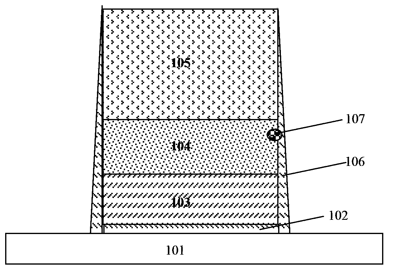
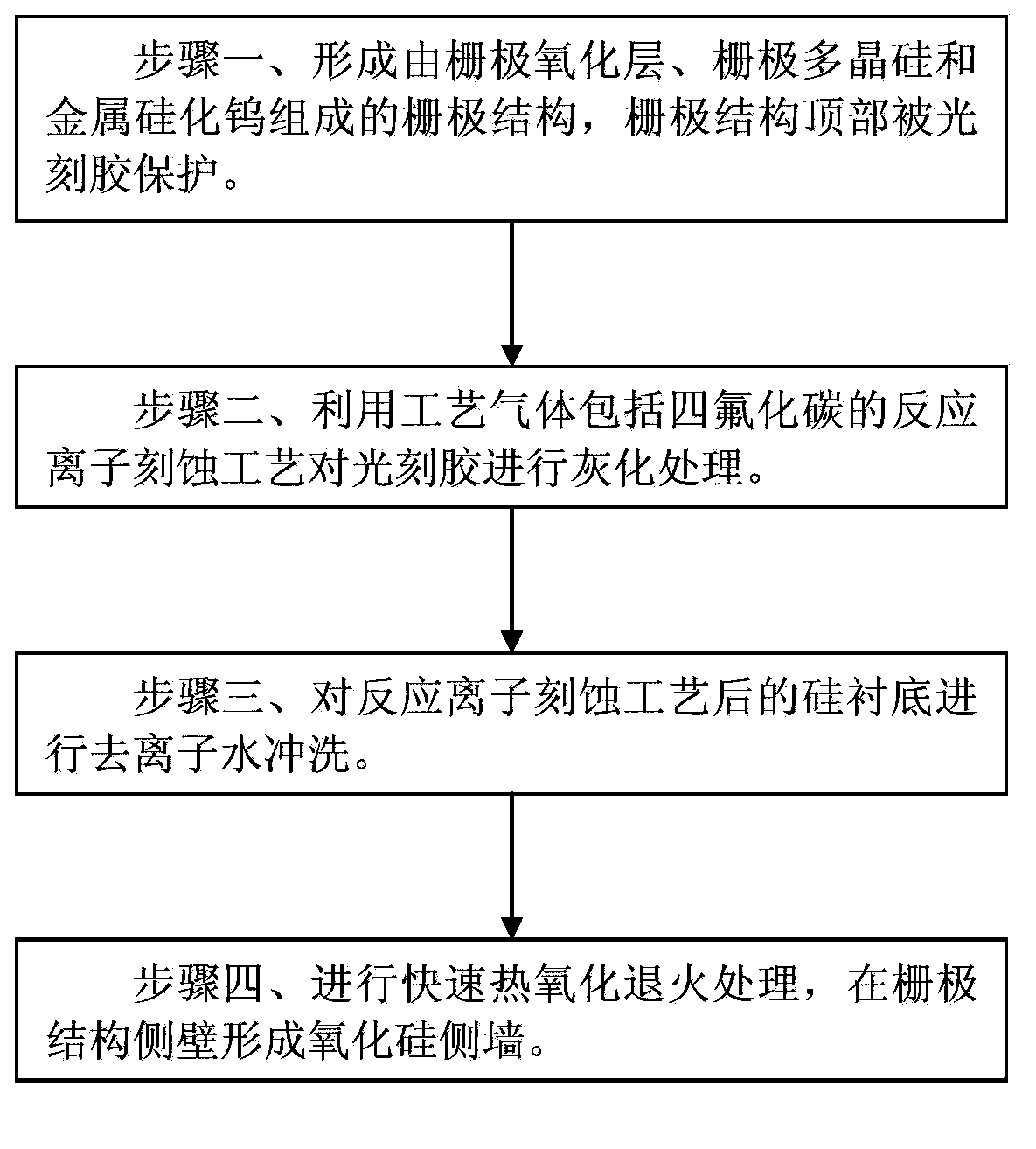
[0018] Such as figure 2 Shown is the flow chart of the method of the embodiment of the present invention; Figure 3A to Figure 3C Shown is a schematic diagram of the device structure in each step of the method of the embodiment of the present invention. The method for forming the silicon oxide sidewall of the metal tungsten silicide gate in the embodiment of the present invention includes the following steps:

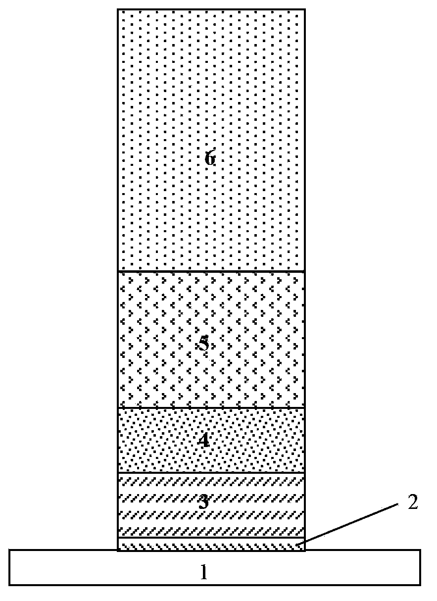
[0019] Step 1, such as Figure 3A As shown, a gate oxide layer 2, gate polysilicon 3, metal tungsten silicide 4 are sequentially formed on the surface of a silicon substrate 1, and a silicon nitride protective layer 5 is formed on the surface of the metal tungsten silicide 4; The photoresist 6 defines the pattern area of ​​the gate structure, and the silicon nitride protection layer 5, the metal tungsten silicide 4, the gate polysilicon 3 and the The gate oxide layer 2 is etched to form a gate structure pattern composed of the gate oxide layer 2, the gate polysilico...


PUM

PropertyMeasurementUnit
thicknessaaaaaaaaaa

Abstract

The invention discloses a method for forming a silicon oxide side wall of the gate of metal tungsten silicide. The method includes the steps that a gate structure composed of gate oxide, gate polycrystalline silicon and the metal tungsten silicide is formed, and the top of the gate structure is protected by photoresist; the RIE process of process gas including carbon tetrafluoride is utilized to conduct ashing processing on the photoresist; a silicon substrate on which the RIE process is conducted is rinsed with deionized water; the RTO process is conducted, and then the silicon oxide side wall is formed on the side wall of the gate structure. By the adoption of the method, grains of the metal tungsten silicide can be prevented from growing to form spherical protrusions when the silicon oxide side wall grows, point discharge caused by the spherical protrusions can also be avoided, and breakdown voltages of devices are increased; in addition, process cost can be reduced. According to the silicon oxide side wall formed through the method, stress between a silicon nitride layer and a gate polycrystalline silicon side wall can be reduced, and lattice defects of the gate polycrystalline silicon side wall can be repaired.

Description

technical field [0001] The invention relates to a semiconductor integrated circuit manufacturing process method, in particular to a method for forming silicon oxide sidewalls of metal tungsten silicide gates. Background technique [0002] In the MOS process of metal tungsten polycide gate (Tungsten Polycide), after the gate pattern is etched, it is necessary to form a layer with a thickness of about The silicon oxide sidewall is used as a protective layer. Such as figure 1 As shown, it is a schematic structural diagram of the silicon oxide sidewall of the metal tungsten silicide gate formed by the existing method; the existing method usually adopts the furnace tube method to grow the silicon oxide sidewall on the sidewall of the gate structure, wherein the gate structure includes The gate oxide layer 102, gate polysilicon 103 and metal tungsten silicide 104 are sequentially formed on the surface of the silicon substrate 101. A silicon nitride protective layer 105 is also ...

Claims


Application Information

Patent Timeline
Patent Type & Authority Applications(China)
IPC IPC(8): H01L21/28H01L21/336
CPCH01L21/28132H01L21/28247H01L29/66568
Inventor 陈瑜马斌陈华伦罗啸
Owner SHANGHAI HUAHONG GRACE SEMICON MFG CORP
Why Eureka
Try Eureka