Area array quad flat no lead package (AAQFN) package body package in package (PiP) piece with solder balls and production method
A technology of leadless packaging and spherical arrays, which is applied in semiconductor/solid-state device manufacturing, electric solid-state devices, semiconductor devices, etc., can solve problems such as unsatisfactory short-term requirements, difficult frame manufacturing process, and long R&D cycle to reduce production The effect of reducing costs and shortening the R&D cycle
- Summary
- Abstract
- Description
- Claims
- Application Information
AI Technical Summary
Problems solved by technology
Method used
Image

Examples
preparation example Construction
[0046] The preparation method of a kind of above-mentioned package that the present invention provides, specifically carries out according to the following steps:
[0047] Step 1: Thinning Scribing:
[0048] Using 8-inch to 12-inch thinning machine, using rough grinding, fine grinding and polishing anti-warping process, the wafer with bump chip is thinned to 180μm-200μm; the rough grinding speed is 6μm / s, and the fine grinding speed is 1.0μm / s; using rough grinding, fine grinding and polishing anti-warping process, the wafer without bumps is thinned to 50 μm ~ 75 μm, the rough grinding speed is 3 μm / s, and the fine grinding speed is 6.0 μm / min; the chip is prevented from warping Qu craft;
[0049] Use the A-WD-300TXB dicing machine to dicing the thinned 8-inch to 12-inch wafers, and the dicing feed speed is ≤10mm / s;
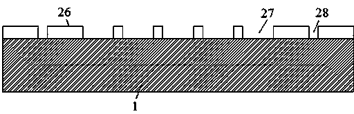
[0050] Step 2: On the dry film placement machine, paste the dry film film 26 on the front of the bare copper frame 1, and bake it at a temperature of 35°C to ...
Embodiment 1
[0067] Using 8-inch to 12-inch thinning machine, adopts rough grinding, fine grinding and polishing anti-warping process, the wafer with bump chip is thinned to 200 μm, the rough grinding speed is 6 μm / s, and the fine grinding speed is 1.0 μm / s ;Using rough grinding, fine grinding and polishing anti-warping process, the wafer without bump chip is thinned to 75 μm, the rough grinding speed is 3 μm / s, and the fine grinding speed is 6.0 μm / min; the chip warping prevention process is adopted; A-WD-300TXB dicing machine is used for scribing, and the scribing speed is ≤10mm / s. Use a dry film sticking machine to stick the dry film on the front of the bare copper frame and bake it at 35°C for 20 minutes. Then, align, expose, develop, and fix the bare copper frame with the dry film on the exposure machine, display the pattern on the bare copper frame, and then harden the film at a temperature of 85°C for 30 minutes; then etch and clean On the machine, by spraying acidic etching soluti...
Embodiment 2
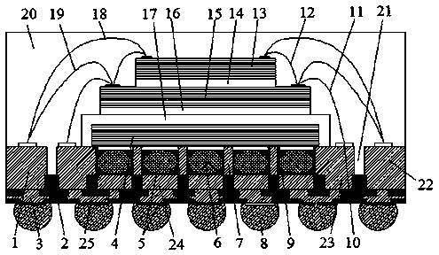
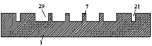
[0069] In the process of wafer thinning and dicing, the final thinning thickness of the wafer with bumps is 180 μm; the final thinning thickness of the wafer without bumps is 50 μm, and the rest are the same as in Example 1; Paste the dry film 26 on the front of the bare copper frame 1, and bake at a temperature of 60°C for 10 minutes; The second groove 27 and the third groove 28 with a pattern are shown on the copper frame 1, and the film is hardened for 35 minutes at a temperature of 80° C.; then a UBM composed of three metal layers is prepared according to the method of Example 1 1 Layer 33 and lead frame pad 10, the three-layer metal layer is the first metal layer, the second metal layer and the third metal layer arranged in sequence, the first metal layer is Ni layer, the second metal layer Cr layer, the third metal layer The metal layer is an Au layer, and the first metal layer is in contact with the bare copper frame 1; then the stacked package with a soldered ball arra...
PUM
 Abstract
Description
Claims
Application Information
 - R&D
- Intellectual Property
- Life Sciences
- Materials
- Tech Scout
- Unparalleled Data Quality
- Higher Quality Content
- 60% Fewer Hallucinations
Browse by: Latest US Patents, China's latest patents, Technical Efficacy Thesaurus, Application Domain, Technology Topic, Popular Technical Reports.
© 2025 PatSnap. All rights reserved.Legal|Privacy policy|Modern Slavery Act Transparency Statement|Sitemap|About US| Contact US: help@patsnap.com