Magnetic element based on spin hall effect, microwave oscillator and manufacturing method thereof

A spin Hall effect, microwave oscillator technology, applied in the fields of magnetic field controlled resistors, the manufacture/processing of electromagnetic devices, material selection, etc., can solve the problem of thermal noise affecting the quality of output microwave signals, high preparation conditions current density and other issues, to achieve the effect of easy mass preparation, simple preparation process and good performance

Inactive Publication Date: 2014-05-07
SUZHOU INST OF NANO TECH & NANO BIONICS CHINESE ACEDEMY OF SCI
View PDF2 Cites 28 Cited by
  • Summary
  • Abstract
  • Description
  • Claims
  • Application Information

AI Technical Summary

Problems solved by technology

However, the spin-polarized current generated by using magnetic materials is restricted by the spin-polarized efficiency. In the process of realizing microwave oscillation, a higher current density is often required, which not only increases energy consumption, but also generates thermal noise. The quality of the output microwave signal, and the spin microwave oscillator based on the spin polarized current, the preparation conditions are relatively high

Method used


Image

  • Magnetic element based on spin hall effect, microwave oscillator and manufacturing method thereof
  • Magnetic element based on spin hall effect, microwave oscillator and manufacturing method thereof
  • Magnetic element based on spin hall effect, microwave oscillator and manufacturing method thereof

Examples


Embodiment 1

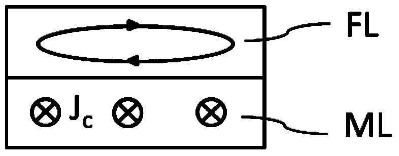
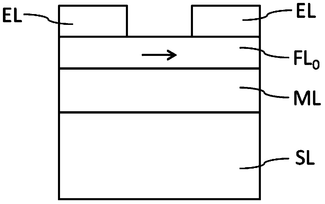
[0057] Embodiment 1 This embodiment relates to a two-terminal microwave oscillator based on the spin Hall effect, which includes: a substrate layer 1; a non-magnetic layer 121 located on the substrate; a magnetic layer 131 located on the non-magnetic layer ; and a metal electrode 141 located on the magnetic layer. Based on this structure, the spin current generated by the spin Hall effect and the anisotropic magnetoresistance effect to generate the oscillating signal are utilized.

[0058] refer to image 3 As shown, in a typical embodiment, the involved device includes a single crystal silicon substrate (Si / SiO 2 ), non-magnetic metal layer (Pt), magnetic film layer (Py) and metal electrode (Au).

[0059] The manufacturing process of the two-terminal device includes:

[0060] First, on Si / SiO 2 A nonmagnetic metal layer 121 (Pt, 2nm) and a magnetic film layer 131 (Py, 1nm) are deposited on the substrate by magnetron sputtering. Then, the pattern structure of the non-magn...

Embodiment 2

[0063] Embodiment 2 This embodiment also relates to a two-terminal microwave oscillator based on the spin Hall effect, which is composed of different materials from Embodiment 1, and the corresponding manufacturing process is also different.

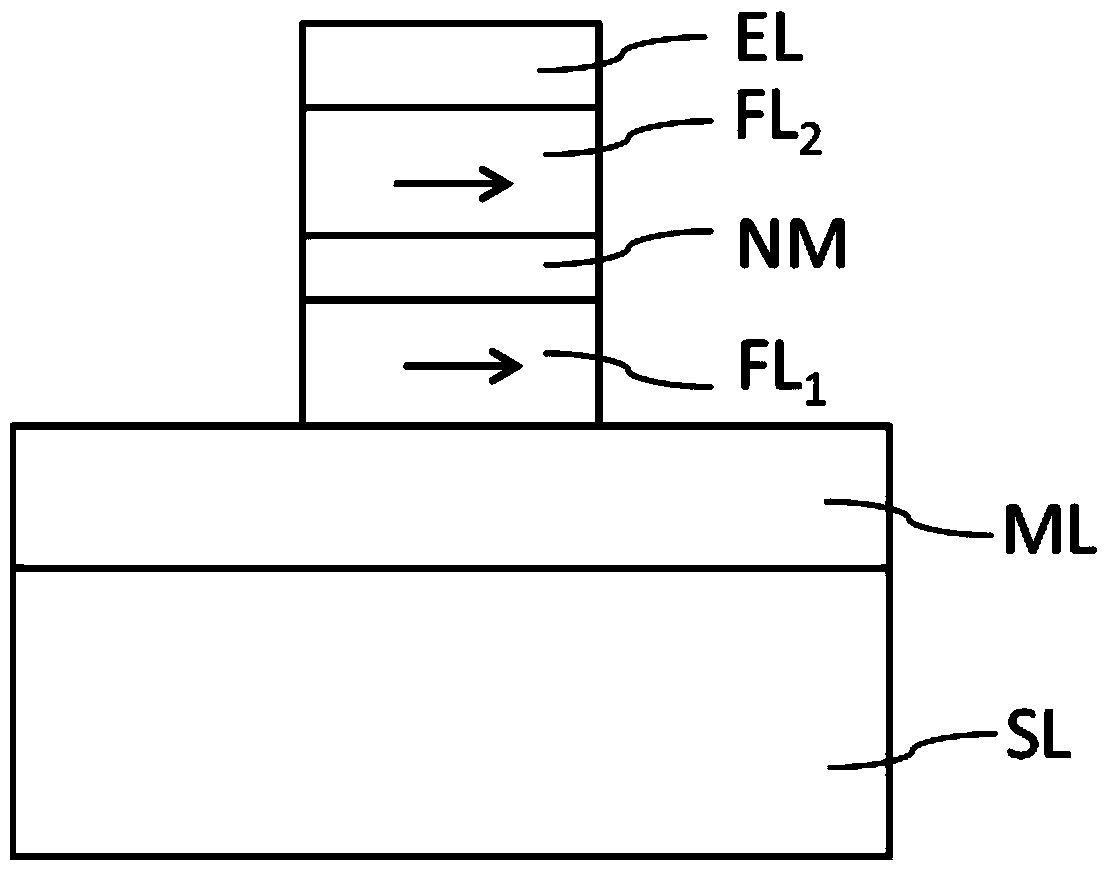
[0064] More specifically, the two-terminal device structure of this embodiment includes: a substrate layer 2; a non-magnetic layer 221 located on the substrate; a magnetic layer 231 located on the non-magnetic layer; and a metal electrode located on the magnetic layer 241. Based on this structure, the spin current generated by the spin Hall effect and the anisotropic magnetoresistance effect to generate the oscillating signal are utilized.

[0065] In a more specific typical embodiment, the device involved includes a single crystal silicon substrate (Si / SiO 2 ), non-magnetic metal layer (Pb), magnetic film layer (YIG) and metal electrode (Cu).

[0066] The manufacturing process of the two-terminal device includes:

[0067] First, take...

Embodiment 3

[0069] Embodiment 3 This embodiment also relates to a two-terminal microwave oscillator based on the spin Hall effect, which is different from Embodiments 1 and 2 in terms of composition and materials, and the corresponding manufacturing process is also different.

[0070] More specifically, the two-terminal device structure of this embodiment includes: a substrate layer 3; a non-magnetic layer 321 located on the substrate; a dilute magnetic semiconductor layer 331 located on the non-magnetic layer; and a metal electrode 341 . Based on this structure, the spin current generated by the spin Hall effect and the anisotropic magnetoresistance effect to generate the oscillating signal are utilized.

[0071] In a more specific typical embodiment, the related device includes a sapphire substrate, a non-magnetic metal layer (W), a magnetic film layer (GaMnAs) and a metal electrode (Au) distributed sequentially along a set direction.

[0072] The manufacturing process of the two-termi...


PUM


Abstract

The invention discloses a magnetic element based on a spin hall effect, a microwave oscillator and a manufacturing method thereof. The magnetic element comprises a non-magnetic metal film layer (ML) and a magnetic film layer (FL), wherein the non-magnetic metal film layer (ML) can induce electrons to generate spin currents, and the magnetic film layer (FL) is formed on the non-magnetic metal film layer (ML) and can balance magnetization. The microwave oscillator comprises the magnetic element, the magnetic element is formed on a substrate layer (SL), and metal electrodes (EL) are formed on the magnetic element. The microwave oscillator can be formed by using a thin film deposit technology, a photoetching and/or etching technology and the like. The structure of the magnetic element is beneficial to reducing the noise of the microwave oscillator, device microwave frequency is wide in adjustable range under the effect of impressed currents, and output microwave signals are excellent in performance. The microwave oscillator has the advantages of being small in size, simple in structure and the like, and is simple in manufacturing technology, compatible with traditional nano-meter processing technologies, easy to manufacture in a mass mode and capable of serving as a microwave source to be widely applied in the fields of electronics, communication and the like.

Description

technical field [0001] The invention particularly relates to a magnetic element based on the spin Hall effect, a microwave oscillator and a manufacturing method thereof, and belongs to the technical field of microwave oscillators. Background technique [0002] A microwave oscillator is an electronic component that converts a DC signal into an AC signal with a certain frequency. It is widely used in the electronics industry, medical treatment, and scientific research. In recent years, with the rapid development of mobile communications and satellite communications, the requirements for the miniaturization and integration of oscillators are becoming more and more urgent. At the same time, mobile communication is also developing towards high frequency and broadband. Currently, commercial oscillators mainly include LC oscillators and crystal oscillators. The circuit design of the commercial LC oscillator is flexible, the cost is low, and it is easy to achieve sine wave output a...

Claims


Application Information

Patent Timeline
Patent Type & Authority Applications(China)
IPC IPC(8): H01L43/08H01L43/10H01L43/12
Inventor 方彬曾中明张宝顺
Owner SUZHOU INST OF NANO TECH & NANO BIONICS CHINESE ACEDEMY OF SCI
Why Eureka
Try Eureka