Isolation structure and formation method thereof

A technology of isolation structure and trench, which is applied in the direction of electrical components, semiconductor/solid-state device manufacturing, circuits, etc., can solve the problems of low deposition efficiency, high cost, and insufficient oxide quality, so as to improve the isolation effect, reduce the difficulty, The effect of improving fill quality

Active Publication Date: 2014-05-14
SEMICON MFG INT (SHANGHAI) CORP
View PDF7 Cites 8 Cited by
  • Summary
  • Abstract
  • Description
  • Claims
  • Application Information

AI Technical Summary

Problems solved by technology

However, the quality of the oxide formed by the FCVD process is

Method used


Image

  • Isolation structure and formation method thereof
  • Isolation structure and formation method thereof
  • Isolation structure and formation method thereof

Examples


no. 1 example

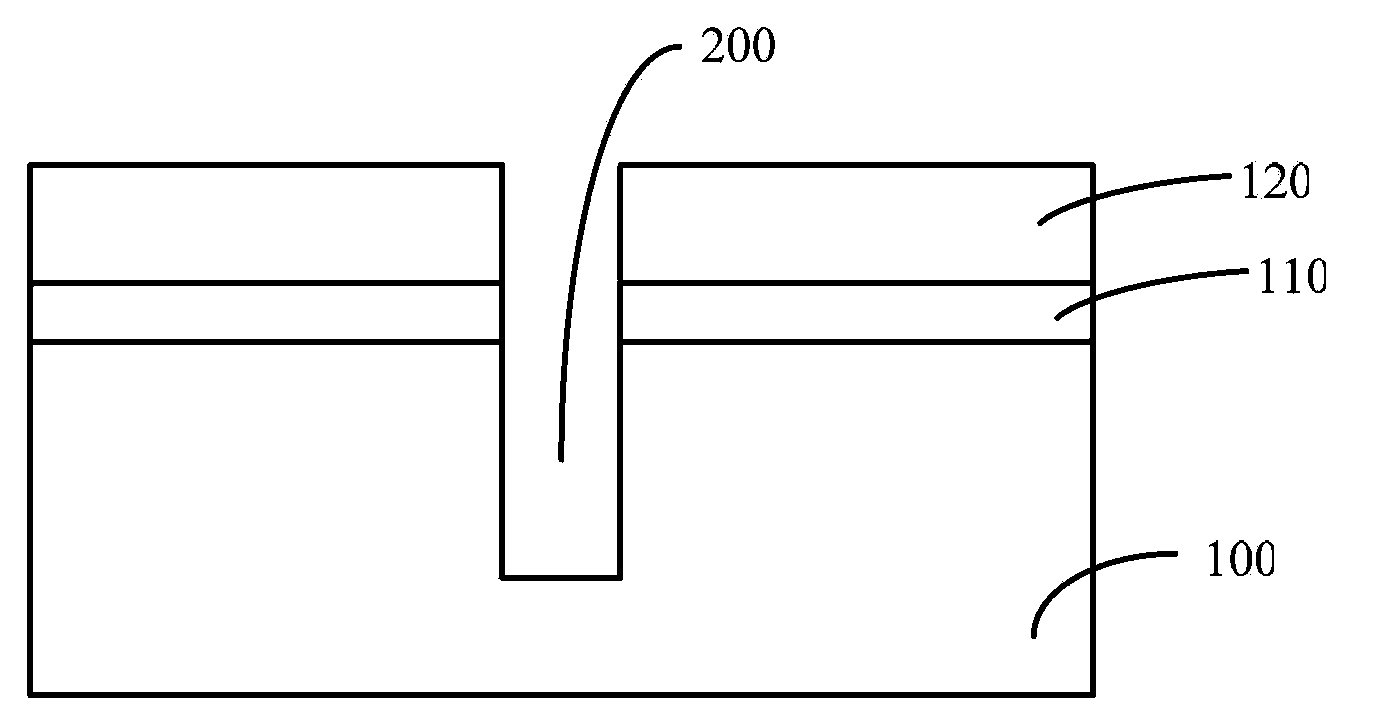
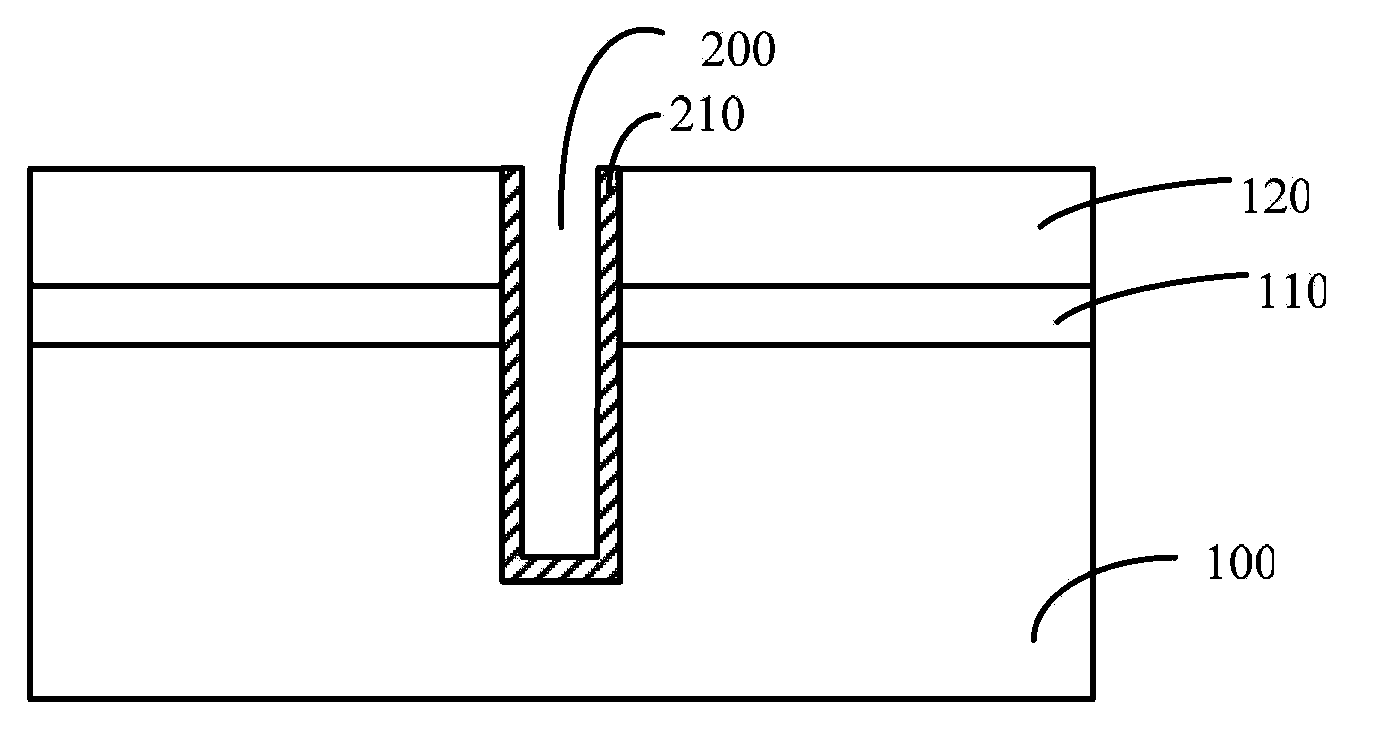
[0035] Please refer to figure 1 A semiconductor substrate 100 is provided, the surface of the semiconductor substrate has a mask layer, and the mask layer includes a silicon oxide layer 110 on the surface of the substrate and a silicon nitride layer 120 on the surface of the silicon oxide layer 110 . Trenches 200 are formed in the semiconductor substrate.

[0036] Specifically, the material of the semiconductor substrate 100 includes semiconductor materials such as silicon, germanium, silicon germanium, and gallium arsenide, and may be a bulk material or a composite structure such as silicon-on-insulator. Those skilled in the art can select the type of the semiconductor substrate 100 according to the semiconductor devices formed on the semiconductor substrate 100 , so the type of the semiconductor substrate should not limit the protection scope of the present invention. In this embodiment, bulk silicon is used as the semiconductor substrate.

[0037]The silicon oxide layer ...

no. 2 example

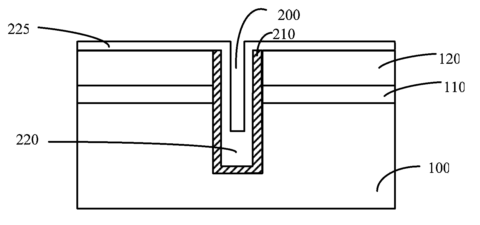
[0059] Please refer to Image 6 , in the second embodiment of the present invention, after forming the second dielectric material in the trench according to the method in the first embodiment, before forming the third dielectric material layer, the sidewalls covering the unfilled upper part of the trench are removed, The side walls of the hard mask layer on both sides of the opening above the groove, and the second dielectric film on the surface of the hard mask layer.

[0060] The process of removing the second dielectric film 225 is wet etching, and the etching solution is HF. The first dielectric layer 210 and the silicon nitride layer 120 are used as an etching stop layer. Specifically, the second dielectric material is annealed first, and after the second dielectric layer 220 and the second dielectric film 225 are formed, the second dielectric film 225 is removed.

[0061]In other embodiments of the present invention, before annealing the second dielectric material, a w...


PUM

PropertyMeasurementUnit
Thicknessaaaaaaaaaa

Abstract

An isolation structure and a formation method thereof are provided. The formation method of the isolation structure comprises the following steps: providing a semiconductor substrate, wherein the surface of the semiconductor substrate is provided with a mask layer; etching the mask layer and the semiconductor substrate and forming a groove in the semiconductor substrate; forming a second dielectric layer in the groove by utilizing fluid chemical vapor deposition (FCVD) process, wherein the second dielectric layer fills partial space at the bottom portion in the groove; and forming a third dielectric layer in the rest space at the upper portion in the groove, the third dielectric layer being located above the second dielectric layer. By utilizing the method in the invention to fill the groove, the appearance of cavities can be effectively prevented, and filling quality of the high aspect ratio groove is improved.

Description

technical field [0001] The invention relates to the technical field of semiconductors, in particular to an isolation structure and a forming method thereof. Background technique [0002] Submicron and smaller feature sizes are one of the key technologies for next-generation VLSI and VLSI of semiconductor devices. The continuous shrinking of dimensions puts forward higher requirements on the formation process of semiconductors, and the formation of high-quality gate patterns and shallow trench isolation (STI) regions is the key to the development of integrated circuits. In order to achieve higher circuit density, not only the feature size of the semiconductor device is reduced, but also the size of the isolation structure between the devices is correspondingly reduced. [0003] Current isolation technologies include Shallow Trench Isolation (STI) processes. The STI process includes: first etching a trench with a certain width and depth on the substrate, then filling the tre...

Claims


Application Information

Patent Timeline
IPC IPC(8): H01L21/762
CPCH01L21/76224
Inventor 洪中山
Owner SEMICON MFG INT (SHANGHAI) CORP
Why Eureka
Try Eureka