Processing method of all metal channel microstructure with great thickness and high depth-to-width ratio

A technology with high aspect ratio and processing method, applied in the direction of microstructure technology, microstructure device, manufacturing microstructure device, etc., can solve the problems of long etching time, difficult control of ion beam, microstructure damage, etc.

Inactive Publication Date: 2014-05-28
HEFEI UNIV OF TECH
View PDF5 Cites 12 Cited by
  • Summary
  • Abstract
  • Description
  • Claims
  • Application Information

AI Technical Summary

Problems solved by technology

[0004] (2) Using deep reactive ion etching technology to prepare structures with large thickness and high aspect ratio, the et

Method used


Image

  • Processing method of all metal channel microstructure with great thickness and high depth-to-width ratio
  • Processing method of all metal channel microstructure with great thickness and high depth-to-width ratio
  • Processing method of all metal channel microstructure with great thickness and high depth-to-width ratio

Examples


Embodiment Construction

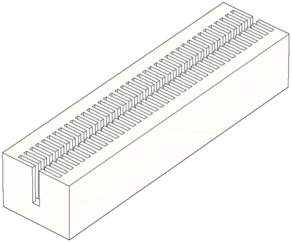
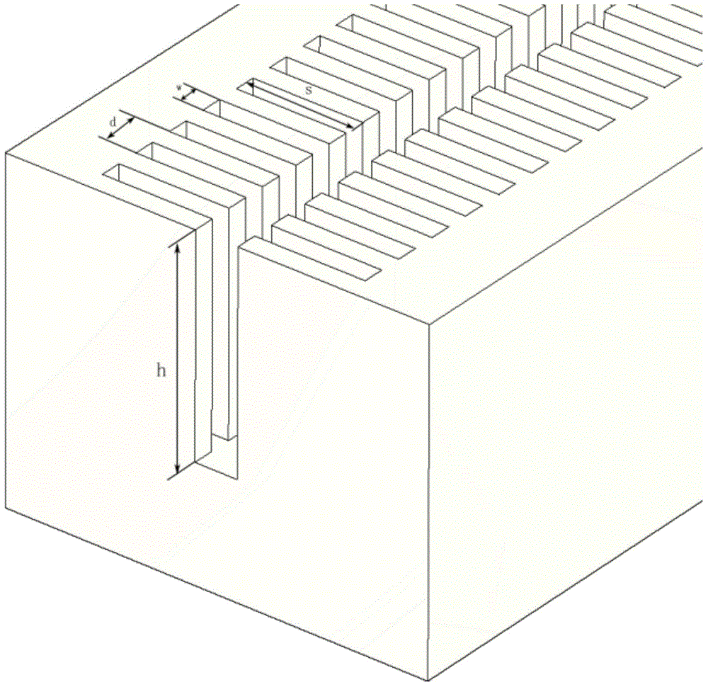
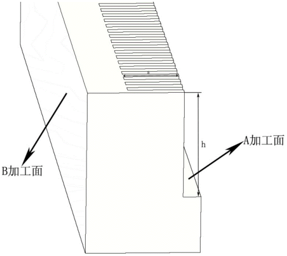
[0029] Such as Figure 1-7 , A method for processing a large-thickness, high-aspect-ratio all-metal trench microstructure, specifically including the following steps:

[0030] (1) Preparation of the substrate, punching, gluing, and preparation of the mask: According to the structural requirements, process the copper substrate of the set size, and process the positioning pin holes at the same position on the different copper sheets; before preparation ,Using ultrasonic cleaning and plasma cleaning to treat the surface of the copper substrate to optimize the cleanliness and surface energy of the substrate surface.

[0031] (2) Ultraviolet lithography: The process of ultraviolet lithography includes spin coating, pre-baking, exposure, post-baking, development and vertical film. The micro electroforming master mold of the single grating is prepared through the above process.

[0032] (3) Micro-electroforming and degumming molding: Put the previously prepared electroforming master mold ...


PUM


Abstract

The invention discloses a processing method of an all metal channel microstructure with great thickness and a high depth-to-width ratio. The processing method comprises the particular technical steps of spin-coating a copper substrate in a set size with a layer of SU-8 photoresist, performing technical procedures such as prebaking, exposing, postbaking, developing, and film upright to form a micro-electroforming female mold, obtaining 1/2 structures by a micro-electroforming and striping technology, and finally, combining the two 1/2 structures into a whole by a pin connection technology. According to the method, the all metal channel microstructure with the great thickness and the high depth-to-width ratio can be obtained by a once gluing technology together with the pin connection technology; the problem in verticality of a side wall caused by exposure and the problem of photoresist residual in a channel caused by incomplete striping when a great thickness glue film is obtained by using the gluing technology for many times are avoided; and a processing bottle neck in the structural thickness and the depth-to-width ratio when the all metal microstructure is prepared by the conventional UV-LIGA (Ultraviolet-Lithographie, Galanoformung and Abformung) technology and the deep reactive ion etching technology are broken through.

Description

Technical field [0001] The invention belongs to the technical field of all-metal microstructure manufacturing, and particularly relates to a method for processing an all-metal channel type microstructure with a large thickness and a high aspect ratio. Background technique [0002] The all-metal channel microstructure has a wide range of applications in the field of terahertz vacuum electronics and microelectromechanical systems. With the development of electronic technology and micro-electromechanical systems, the size of all-metal channel microstructures has also changed correspondingly, from the nanometer and micrometer levels that can be achieved by traditional micro-nano processing to the size level of 100 microns. The size level of 100μm-1mm is the technical gap between the traditional mechanical processing field and the current microprocessing field. At present, the UV-LIGA technology based on SU-8 thick photoresist and the deep reactive ion etching technology have microstr...

Claims


Application Information

Patent Timeline
IPC IPC(8): B81C1/00
Inventor 阮久福邓光晟卢怡如张称单云冲杨军
Owner HEFEI UNIV OF TECH
Why Eureka
Try Eureka