

Epitaxial growth method capable of improving anti-static electricity capacity of III-V class compound semiconductor LED (light emitting diode) chip
An LED chip, epitaxial growth technology, applied in crystal growth, semiconductor devices, chemical instruments and methods, etc., can solve the problems of thermal expansion coefficient difference, lattice defect stress, excessive local current, etc., to reduce piezoelectric field effect, The effect of avoiding breakdown and improving the ability of antistatic
- Summary
- Abstract
- Description
- Claims
- Application Information
AI Technical Summary
Problems solved by technology
Method used
Image

Examples
Embodiment 1
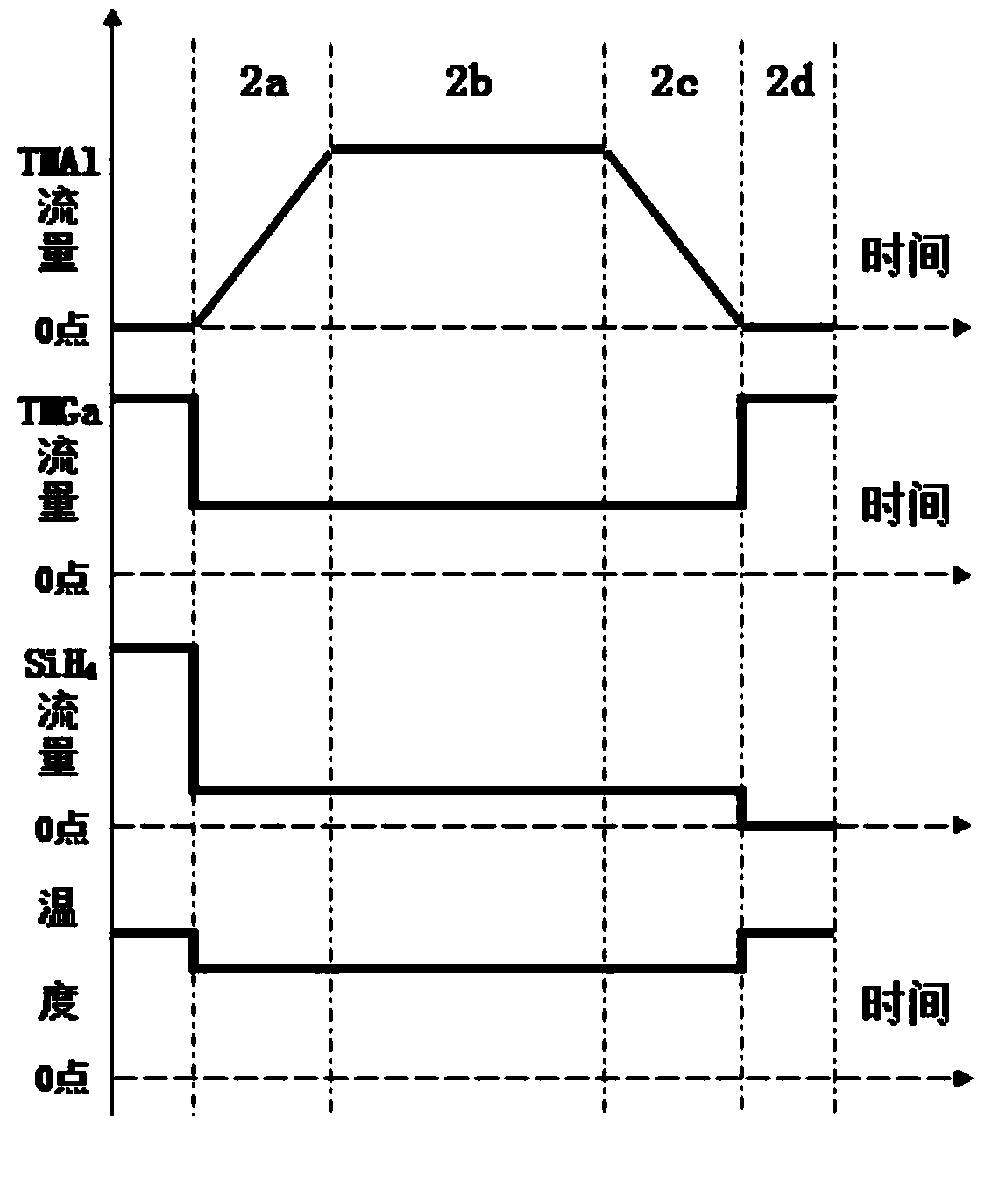
[0026] An epitaxial growth method for improving the antistatic ability of III-V compound semiconductor LED chips. The LED epitaxial structure includes, from bottom to top, a substrate, a GaN buffer layer, a GaN undoped layer, and an N-type doped layer. GaN layer, shallow well layer, n-type AlGaN / GaN composite insertion layer, multi-quantum well active layer, low-temperature P-type GaN layer, P-type AlGaN layer, high-temperature P-type GaN layer, and P-type contact layer. The growth methods specifically include The following steps:
[0027] (1) Sapphire (Al 2 o 3 ) The substrate is subjected to high-temperature cleaning treatment in a hydrogen atmosphere at 1000°C for 5 minutes, and then nitriding treatment;
[0028] (2) Sapphire (Al 2 o 3 ) After the high-temperature treatment of the substrate is completed, the temperature is lowered to 500°C, and a GaN buffer layer with a thickness of 20nm is grown at a growth pressure of 400Torr and a V / III ratio of 50;
[0029](3) Afte...
Embodiment 2
[0041] An epitaxial growth method for improving the antistatic ability of III-V compound semiconductor LED chips. The LED epitaxial structure includes, from bottom to top, a substrate, a GaN buffer layer, a GaN undoped layer, and an N-type doped layer. GaN layer, shallow well layer, n-type AlGaN / GaN composite insertion layer, multi-quantum well active layer, low-temperature P-type GaN layer, P-type AlGaN layer, high-temperature P-type GaN layer, and P-type contact layer. The growth methods specifically include The following steps:
[0042] (1) Sapphire (Al 2 o 3 ) The substrate is subjected to a high-temperature cleaning treatment in a hydrogen atmosphere at 1200°C for 20 minutes, and then to a nitriding treatment;
[0043] (2) Sapphire (Al 2 o 3 ) After the high-temperature treatment of the substrate is completed, the temperature is lowered to 650°C, and a GaN buffer layer with a thickness of 40nm is grown, the growth pressure is 600Torr, and the V / III ratio is 500;
[0...
Embodiment 3
[0056] An epitaxial growth method for improving the antistatic ability of III-V compound semiconductor LED chips. The LED epitaxial structure includes, from bottom to top, a substrate, a GaN buffer layer, a GaN undoped layer, and an N-type doped layer. GaN layer, shallow well layer, n-type AlGaN / GaN composite insertion layer, multi-quantum well active layer, low-temperature P-type GaN layer, P-type AlGaN layer, high-temperature P-type GaN layer, and P-type contact layer. The growth methods specifically include The following steps:
[0057] (1) Sapphire (Al 2 o 3) Substrate 1 is subjected to high-temperature cleaning treatment in a hydrogen atmosphere at 1100°C for 15 minutes, and then to nitriding treatment;
[0058] (2) Sapphire (Al 2 o 3 ) After the high-temperature treatment of the substrate is completed, the temperature is lowered to 550°C to grow a GaN buffer layer with a thickness of 30nm, the growth pressure is 500Torr, and the V / III ratio is 400;
[0059] (3) Afte...
PUM
| Property | Measurement | Unit |
|---|---|---|
| Thickness | aaaaa | aaaaa |
| Thickness | aaaaa | aaaaa |
| Thickness | aaaaa | aaaaa |
Abstract
Description
Claims
Application Information