Absorbing film structure based on visible band to near-infrared band

A near-infrared and absorbing film technology, applied in the field of absorbing films, can solve the problems that it is difficult to etch a large area of ​​the metal surface, hinder the near-perfect absorption of near-infrared specific bands, and achieve low cost, high coordination and simple process. Effect

Inactive Publication Date: 2014-06-11
SHANGHAI INST OF TECHNICAL PHYSICS - CHINESE ACAD OF SCI
View PDF6 Cites 10 Cited by
  • Summary
  • Abstract
  • Description
  • Claims
  • Application Information

AI Technical Summary

Problems solved by technology

To achieve near-perfect absorption in the visible to near-infrared band, the periodic structure of the material surface must be in the range of hundreds of nanometers. It is difficult to etch a large area with a small period and high precision on the metal surface. In addition, this Etching requires a very flat surface, which has become a major obstacle to the development of near-perfect absorption technology in the visible to near-infrared specific band

Method used


Image

  • Absorbing film structure based on visible band to near-infrared band
  • Absorbing film structure based on visible band to near-infrared band

Examples


Embodiment 1

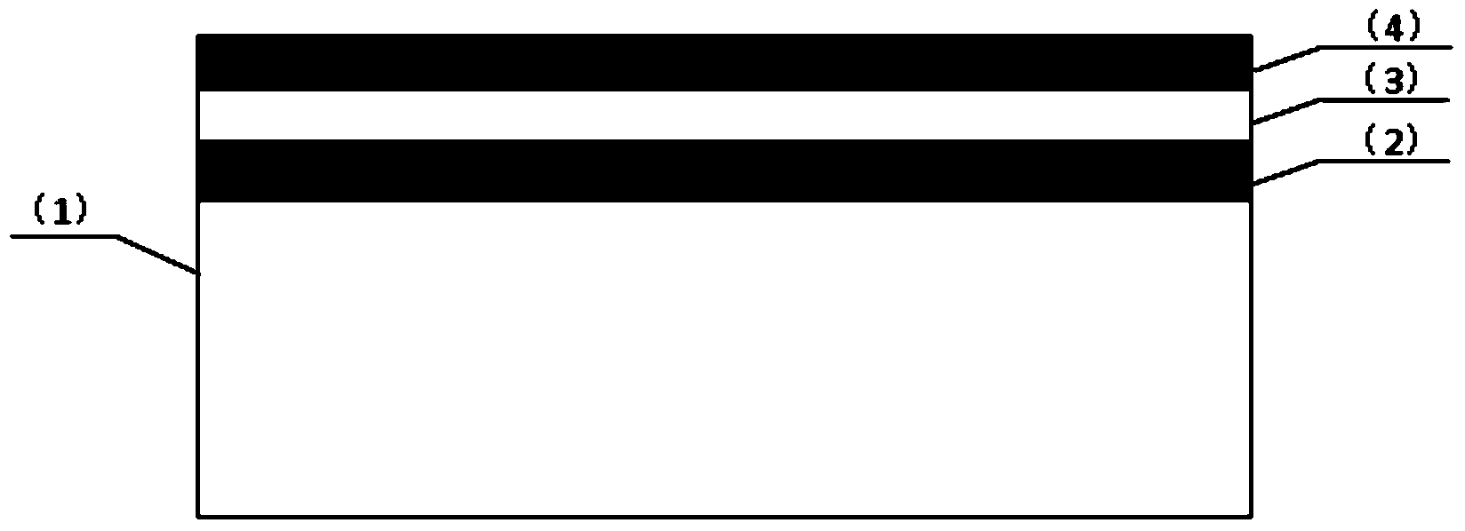
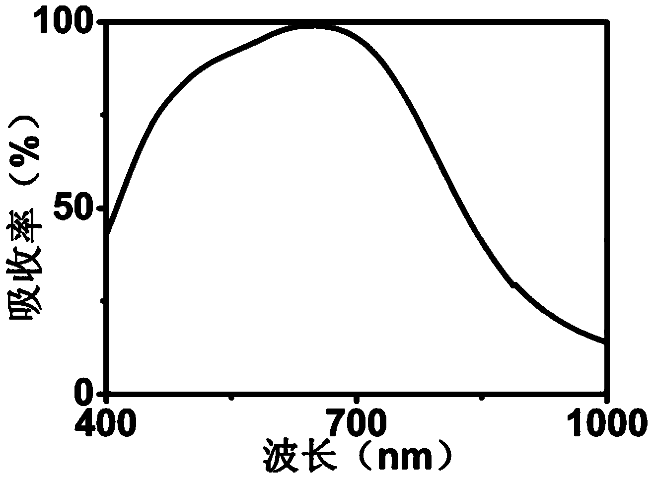
[0014] Sputter a 200nm silver film on a silicon substrate sequentially with an argon ion beam, deposit a 50nm thick zinc oxide film on the silver film by metal-organic chemical vapor phase method, and then sputter on the zinc oxide film by magnetron sputtering 3nm gold thin film, and finally put the multilayer film structure into an environment of 300°C for half an hour to form a thin film layer with randomly distributed gold particles on the surface, with an average height of 25nm, an average size of 50nm, and a surface coverage of 22%. Finally, a multi-layer film structure with near-perfect absorption characteristics in visible to near-infrared bands is obtained.

Embodiment 2

[0016] On the quartz substrate, a 1 μm copper film was deposited sequentially by electroplating, and a 200nm-thick polyelectrolyte film was spin-coated on the silver film by the sol-gel method. In an argon ion beam sputtering instrument, a 60mA current was used to bombard the silver target for 3s on the polyelectrolyte. The silver particle layer is sputtered on the thin film, and the obtained silver particle layer has an average height of 10nm, an average particle size of 60nm, and a surface coverage of 90%. Finally, a multi-layer film structure with near-perfect absorption characteristics in visible to near-infrared bands is obtained.

Embodiment 3

[0018] On the glass substrate, 80nm gold thin film was sequentially deposited by thermal evaporation, and 1nm aluminum oxide thin film was grown on the silver thin film by atomic layer deposition method. Finally, copper particles were adsorbed on the aluminum oxide thin film by electrostatic adsorption method. The height is 100nm, the average particle size is 200nm, and the surface coverage is 3%. Finally, a multi-layer film structure with near-perfect absorption characteristics in visible to near-infrared bands is obtained.


PUM

PropertyMeasurementUnit
thicknessaaaaaaaaaa
thicknessaaaaaaaaaa
thicknessaaaaaaaaaa

Abstract

The invention discloses an absorbing film structure based on visible band to near-infrared band. The absorbing film structure is characterized in that a metal film layer and a dielectric film layer successively grow on any substrate by gas phase deposition and liquid phase deposition, and then an unordered metal particle distribution layer grows on the dielectric film layer by gas phase deposition or a combination of gas phase deposition and an annealing process, wherein the thickness of the metal film layer is 80nm-1micron, the thickness of the dielectric film layer is 1nm-200nm, the average height of an equivalent film layer in the unordered metal particle distribution layer is 5nm-100nm, the average size of particles is 10nm-200nm, and the surface coverage rate of metal particles is 3%-90%. Therefore, the absorbing film structure based on visible band to near-infrared band has a near perfect absorbing characteristic that the absorptivity within visible band to near-infrared band achieves 99%. The absorbing film structure provided by the invention has the advantages that the technology is simple, the cost is low, the modification is not sensitive, the angle is not sensitive, the controllability is good, the coordination is high, the absorbing film structure can grow in a large area manner and has no requirement on a substrate, and the nanometer process technology is ripe.

Description

technical field [0001] The invention relates to an absorption film, specifically referring to a multilayer film system structure of a metal thin film layer-dielectric thin film layer-metal particle random distribution layer. Background technique [0002] With the rapid development of information technology, electromagnetic materials have more and more extensive and profound influence on the current information, national defense, economy, medicine and other fields. In recent years, near-perfect absorption in new artificial electromagnetic materials has attracted more and more attention and has been applied in fields such as thermal radiators, detectors, sensors, photovoltaics, and spatial resolution. The invention proposes a preparation method of a multi-layer periodic film system that can be used in the fields of detectors, space resolution, etc., aiming at the near-perfect absorption technology in the infrared band. [0003] For a long time, etching periodic structures on ...

Claims


Application Information

Patent Timeline
Patent Type & Authority Applications(China)
IPC IPC(8): B32B15/04
Inventor 张云陈鑫孙艳魏调兴董文静张克难戴宁
Owner SHANGHAI INST OF TECHNICAL PHYSICS - CHINESE ACAD OF SCI
Why Eureka
Try Eureka