Equipment for preparing gate dielectric layer

A gate dielectric layer and equipment technology, applied in semiconductor/solid-state device manufacturing, electrical components, circuits, etc., can solve problems such as volatilization and negative impact on carrier migration speed

Inactive Publication Date: 2014-06-11
SHANGHAI HUALI MICROELECTRONICS CORP
View PDF4 Cites 10 Cited by
  • Summary
  • Abstract
  • Description
  • Claims
  • Application Information

AI Technical Summary

Problems solved by technology

[0018] In the above preparation process, since the concentration of nitrogen atoms doped in the gate dielectric layer is high and mainly distributed on the upper surface of the gate dielectric layer, the temperature, gas atmosphere and time interval of the subsequent PNA process must be strictly controlled to prevent the gate dielectric The influence of the intrinsic oxide layer and organic adsorption in the layer on nitrogen doping; in addition, the high-temperature annealing process of PNA (Post Nitridation Anneal) can easily cause the volatilization of nitrogen atoms on the surface, and cause the nitrogen atoms to gain energy and continue to diffuse. cause some nitrogen atoms to accumulate in SiO 2 / Si interface, thus negatively affecting the mobility of carriers in the channel

Method used


Image

  • Equipment for preparing gate dielectric layer
  • Equipment for preparing gate dielectric layer
  • Equipment for preparing gate dielectric layer

Examples


Embodiment Construction

[0040] Embodiments embodying the features and advantages of the present invention will be described in detail in the following description. It should be understood that the invention can have various changes in different examples without departing from the scope of the invention, and that the descriptions and illustrations therein are illustrative in nature rather than limiting the invention.

[0041] The following is attached Figure 3-4, the device for preparing a gate dielectric layer of the present invention will be further described in detail through specific examples. It should be noted that the drawings are all in a very simplified form, using imprecise scales, and are only used to facilitate and clearly achieve the purpose of assisting in describing the embodiments of the present invention.

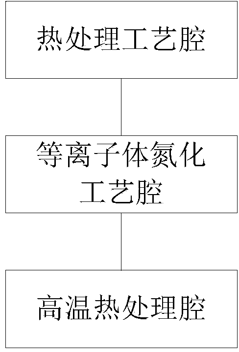
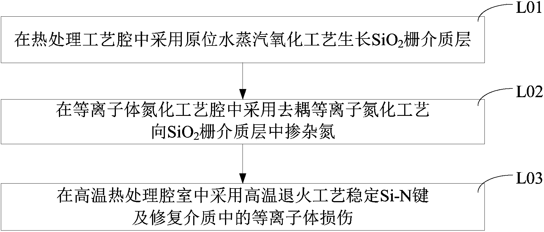
[0042] As mentioned above, the traditional equipment for preparing the gate dielectric layer includes the heat treatment process chamber for growing the gate dielectric by the IS...


PUM


Abstract

The invention provides equipment for preparing a gate dielectric layer. The equipment comprises a thermal treatment process cavity used for growing a SiO2 gate dielectric layer, a plasma nitriding process cavity used for performing plasma nitrogen injection on the gate dielectric layer to form a Si-N bond, a high-temperature nitriding cavity used for repairing lattice damage in the gate dielectric layer and stabilizing the Si-N bond, a low-temperature oxidizing cavity used for repairing a gate dielectric layer/channel interface, a control unit used for controlling conversion of a semiconductor substrate among all the process cavities and opening/closing of all the process cavities, and a conveying device used for conveying the semiconductor substrate among all the process cavities. By adopting a process for preparing the gate dielectric layer in the equipment provided by the invention, the Si-N bond tends to be stable to prevent the volatilization of N atoms, the N concentration in a SiON gate dielectric is stabilized, the dielectric constant of the SiON gate dielectric is increased, reduction of a carrier mobility caused by interface defect is avoided, and the interface quality and the performance of a device are improved.

Description

technical field [0001] The invention relates to the technical field of semiconductor manufacturing, in particular to a device for preparing a gate dielectric layer. Background technique [0002] The rapid development of Very Large Scale Integration (VLSI) and Ultra Large Scale Integration (ULSI) has put forward more special requirements for device processing technology. Among them, the requirement for gate oxide layer when the feature size of MOS devices enters the nanometer era is an obvious challenge. The preparation process of the gate dielectric layer is a key technology in the semiconductor manufacturing process, which directly affects and determines the electrical characteristics and reliability of the device. [0003] The key performance indicator of MOSFET devices is the drive current, and the magnitude of the drive current depends on the gate capacitance. The gate capacitance is proportional to the surface area of ​​the gate and inversely proportional to the thickn...

Claims


Application Information

Patent Timeline
Patent Type & Authority Applications(China)
IPC IPC(8): H01L21/336H01L21/67
CPCH01L29/42364H01L21/3105H01L21/67155
Inventor 张红伟
Owner SHANGHAI HUALI MICROELECTRONICS CORP
Why Eureka
Try Eureka