Chip-level atomic clock air chamber and manufacturing method thereof

A chip-level atomic clock and gas chamber technology, applied to instruments using atomic clocks, can solve the problems of unfavorable atomic clock stability, large gas chamber volume, and increased complexity, and achieve simple and reasonable gas chamber structure, small volume, and simple use Effect

Inactive Publication Date: 2014-06-25
SUZHOU UNIV
View PDF4 Cites 11 Cited by
  • Summary
  • Abstract
  • Description
  • Claims
  • Application Information

AI Technical Summary

Problems solved by technology

[0004] Chinese patent applications CN102491259A and CN102807188A all disclose a MEMS miniature atomic cavity; the microatomic cavity is a gas chamber, comprising a silicon substrate and a borosilicate glass assembly disc, and the glass microcavity formed on the surface of the borosilicate glass assembly disc and the The silicon substrate is bonded to form a closed glass atomic cavity, which is filled with the necessary materials for the atomic clock, and a light incident plane is provided on the side of the glass micro cavity; however, the method first needs to prepare the required glass atomic cavity. The air chamber is prepared, and the volume of the air chamber produced by this scheme is relatively large
[0005] Chinese patent application CN102323738A discloses a trough-type atomic gas chamber, which is formed by bonding a silicon chip with a trough and a Pyrex glass sheet to form a cavity structure; the cavity structure is used for filling alkali metal atom vapor and buffer gas; the trough The cross-section of the groove is an inverted trapezoid; the groove includes a bottom surface and a side wall forming an angle with the bottom surface; although this method uses a critical electrostatic bonding, the path of the air chamber prepared by it is tortuous during use, which increases the subsequent The complexity of use is not conducive to the stability of atomic clocks

Method used


Image

  • Chip-level atomic clock air chamber and manufacturing method thereof

Examples


Embodiment 1

[0027] Embodiment 1: A chip-scale atomic clock gas chamber

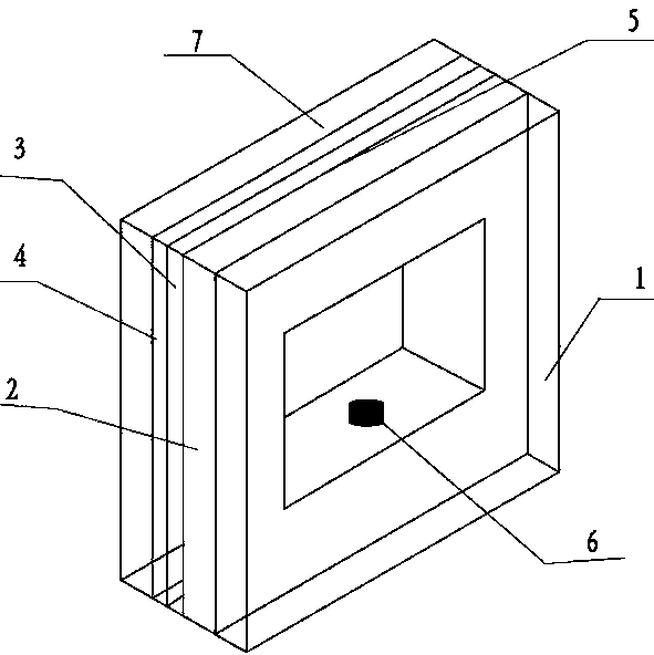
[0028] attached figure 1 The schematic diagram of the structure of the chip-scale atomic clock gas chamber provided for this embodiment; see the attached figure 1 , the chip-level atomic clock gas chamber includes glass 1, SOI silicon wafer 5, alkali metal rubidium 6 and support layer 7, which is a support layer-SOI silicon wafer-glass structure, and the substrate layer 2 of the SOI silicon wafer 5 has a cavity as a cavity Groove, alkali metal rubidium 6 is placed in the groove and filled with inert gas; the substrate layer 2 of the SOI silicon wafer is connected to the glass 1 through electrostatic bonding; the device layer 4 side of the SOI silicon wafer is spin-coated with epoxy resin as a support Layer 7.

[0029] The specific preparation method is as follows:

[0030] (1) RCA standard cleaning steps are used to clean SOI silicon wafers; thermally oxidize and grow oxide layers on both sides of the cleaned sili...

Embodiment 2

[0034] Example 2: Preparation of a chip-scale atomic clock gas chamber

[0035] (1) RCA standard cleaning steps are used to clean SOI silicon wafers; thermally oxidize and grow oxide layers on both sides of the cleaned silicon wafers, and deposit silicon nitride on the oxide layers by LPCVD; The bottom side is photolithographically etched, silicon nitride and silicon oxide are etched to expose part of the silicon wafer, and the silicon wafer without silicon nitride and silicon oxide protection is removed by single-sided KOH wet etching, until the buried layer of the SOI silicon wafer is removed. Thereby preparing a groove as a cavity;

[0036] (2) In the glove box, in a nitrogen atmosphere, place the alkali metal cesium in the groove;

[0037] (3) In the bonding equipment, in an argon atmosphere, conduct silicon-glass electrostatic bonding on the side of the SOI silicon wafer with the substrate through electrostatic bonding, and the cavity has been sealed so far;

[0038] (4...

Embodiment 3

[0039] Example 3: Preparation of a chip-scale atomic clock gas chamber

[0040](1) RCA standard cleaning steps are used to clean SOI silicon wafers; thermally oxidize and grow oxide layers on both sides of the cleaned silicon wafers, and deposit silicon nitride on the oxide layers by LPCVD; The bottom side is photolithographically etched, silicon nitride and silicon oxide are etched to expose part of the silicon wafer, and the silicon wafer without silicon nitride and silicon oxide protection is removed by single-sided KOH wet etching, until the buried layer of the SOI silicon wafer is removed. Thereby preparing a groove as a cavity;

[0041] (2) In the glove box, in a nitrogen atmosphere, place cesium chloride and barium nitride in the groove;

[0042] (3) In the bonding equipment, in the argon / nitrogen mixed gas with a volume ratio of 1:1.4, the silicon-glass electrostatic bonding is carried out on the side of the above-mentioned SOI silicon wafer with the substrate by elec...


PUM

PropertyMeasurementUnit
thicknessaaaaaaaaaa
thicknessaaaaaaaaaa
thicknessaaaaaaaaaa

Abstract

The invention discloses a chip-level atomic clock air chamber and a manufacturing method thereof. An SOI silicon chip is used, a cavity is manufactured on a silicon layer used as a substrate and is used for placing of alkali metal and inflating of inert gas, glass is used for sealing the cavity, finally supporting materials are arranged on one side of a silicon layer used as a device layer to protect a device, and accordingly manufacturing of the high-stability chip-level atomic clock air chamber is completed. Only by one-time key static bonding, manufacturing of the atomic clock air chamber can be completed, the problem of bad stability due to poor static bonding quality is avoided, and finished product rate is improved. The air chamber is simple and reasonable in structure, so that the manufactured air chamber is small in size, easy to use, low in manufacturing cost and suitable for industrial production.

Description

technical field [0001] The invention relates to a chip-level atomic clock gas chamber and a preparation method thereof, belonging to the technical field of atomic clock equipment. Background technique [0002] At present, the atomic clock is the most accurate artificial clock. According to reports, the newly developed atomic clock has an accuracy of 10 to the 18th power. A special type of quantum transition in atomic clocks is the hyperfine transition, which involves the interaction of the nuclear magnetic field of the atom and the magnetic field of the electrons outside the nucleus. At present, atomic clocks are mainly developing in two aspects: one is to improve the accuracy of atomic clocks; the other is to miniaturize them under the premise of ensuring their performance, so as to meet the urgent needs of GPS and communication satellites for atomic clocks. Therefore, how to reduce the size and weight, reduce its power consumption, and have high accuracy and stability are...

Claims


Application Information

Patent Timeline
Patent Type & Authority Applications(China)
IPC IPC(8): G04F5/14
Inventor 张忠山乔东海汤亮韩胜男季磊栗新伟
Owner SUZHOU UNIV
Why Eureka
Try Eureka