Eureka AIR delivers breakthrough ideas for toughest innovation challenges, trusted by R&D personnel around the world.

InAs/GaSb superlattice infrared photoelectric detector and manufacturing method thereof

An electrical detector and superlattice technology, applied in circuits, electrical components, semiconductor devices, etc., can solve the problems of insignificant sidewall undercut effect of etching steps, affecting the photoelectric performance of detectors, and increasing surface tunneling current. , to achieve the effect of suppressing recombination dark current and tunneling dark current, reducing leakage current and improving photoelectric performance

Active Publication Date: 2014-06-25
INST OF SEMICONDUCTORS - CHINESE ACAD OF SCI
View PDF3 Cites 43 Cited by
  • Summary
  • Abstract
  • Description
  • Claims
  • Application Information

AI Technical Summary

Problems solved by technology

[0005] (1) When InAs / GaSb superlattice grows, due to the 7% strain of InAs and GaSb, there is a large stress when the superlattice layer grows, and there is also stress between the superlattice layer and the substrate layer, which seriously affects The growth quality of the material causes a large number of growth defects in the superlattice material, which becomes the main source of a compound dark current and tunneling dark current generated by the detector.
[0006] (2) For the immature wet etching process of the superlattice containing AlSb, the undercut effect of the side wall of the etching step is not obvious, and deposits are easy to adhere, resulting in a large surface leakage current of the device;
[0007] (3) For InAs / GaSb superlattice infrared photodetectors containing AlSb, there are many device passivation steps, and the process is difficult to realize. In addition, oxides are easy to form on the surface of the device during the passivation process, thereby further increasing the surface tunneling current , affecting the photoelectric performance of the detector

Method used

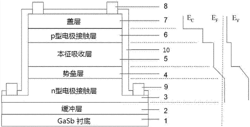
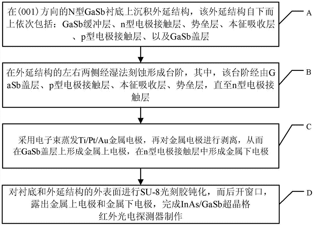
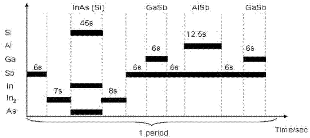

Image

  • InAs/GaSb superlattice infrared photoelectric detector and manufacturing method thereof
  • InAs/GaSb superlattice infrared photoelectric detector and manufacturing method thereof
  • InAs/GaSb superlattice infrared photoelectric detector and manufacturing method thereof

Examples


Embodiment Construction

[0027] In order to make the object, technical solution and advantages of the present invention clearer, the present invention will be described in further detail below in conjunction with specific embodiments and with reference to the accompanying drawings. It should be noted that, in the drawings or descriptions of the specification, similar or identical parts all use the same figure numbers. Implementations not shown or described in the accompanying drawings are forms known to those of ordinary skill in the art. Additionally, while illustrations of parameters including particular values ​​may be provided herein, it should be understood that the parameters need not be exactly equal to the corresponding values, but rather may approximate the corresponding values ​​within acceptable error margins or design constraints. The directional terms mentioned in the embodiments, such as "upper", "lower", "front", "rear", "left", "right", etc., are only referring to the directions of the...


PUM


Abstract

The invention provides an InAs / GaSb superlattice infrared photoelectric detector and a manufacturing method thereof. The InAs / GaSb superlattice infrared photoelectric detector comprises a substrate, an epitaxy structure deposited on the substrate, an upper metal electrode formed above steps, a lower metal electrode formed under the steps and a passivation layer, wherein the epitaxy structure comprises an n-type doping buffer layer, an n-type electrode contact layer, a barrier layer, an intrinsic absorption layer, a p-type electrode contact layer and a cover layer, the steps are formed on two sides of the epitaxy structure through etching, the intrinsic absorption layer is composed of a plurality of periodical InAs / InSb / GaSb / InSb superlattice structures. In the InAs / GaSb superlattice infrared photoelectric detector, InSb is respectively inserted into two interfaces of each superlattice period of the intrinsic absorption layer to form strained superlattices, the stress between the superlattices and the substrate is effectively balanced, the material growing quality is improved, and accordingly the photoelectric performance of the detector is improved.

Description

technical field [0001] The invention relates to the technical field of photoelectric device preparation, in particular to an InAs / GaSb superlattice infrared photodetector and a preparation method thereof. Background technique [0002] With the advancement of science and technology, infrared detectors with military use as the core have gradually developed. Atmospheric monitoring and other military and civilian fields have a wide range of applications. However, the most commonly used silicon-doped detectors, InSb, QWIP, MCT and other infrared detectors are required to work at low temperatures, require special refrigeration equipment, and are expensive, so their applications are limited. The InAs / GaSb infrared detector is due to the particularity of its materials, for example: the high effective mass of electrons and holes can effectively reduce the tunneling current and increase the density of states; the energy difference between the heavy hole band and the light hole band i...

Claims


Application Information

Patent Timeline
Patent Type & Authority Applications(China)
IPC IPC(8): H01L31/102H01L31/036H01L31/0352H01L31/18
CPCH01L31/0304H01L31/035236H01L31/102H01L31/184Y02P70/50
Inventor 蒋洞微向伟王娟邢军亮王国伟徐应强任正伟贺振宏牛智川
Owner INST OF SEMICONDUCTORS - CHINESE ACAD OF SCI
Why Eureka
Eureka Blog
Learn More