Micro-fluidic chip and micro-fluidic chip system for single cell analysis and single cell analyzing method

A microfluidic chip and single-cell technology, applied in the field of single-cell analysis

Active Publication Date: 2014-07-02
THE NAT CENT FOR NANOSCI & TECH NCNST OF CHINA
View PDF10 Cites 82 Cited by
  • Summary
  • Abstract
  • Description
  • Claims
  • Application Information

AI Technical Summary

Problems solved by technology

That is to say, there is no report on a microfluidic chip for single cell an

Method used


Image

  • Micro-fluidic chip and micro-fluidic chip system for single cell analysis and single cell analyzing method
  • Micro-fluidic chip and micro-fluidic chip system for single cell analysis and single cell analyzing method
  • Micro-fluidic chip and micro-fluidic chip system for single cell analysis and single cell analyzing method

Examples


Embodiment 1

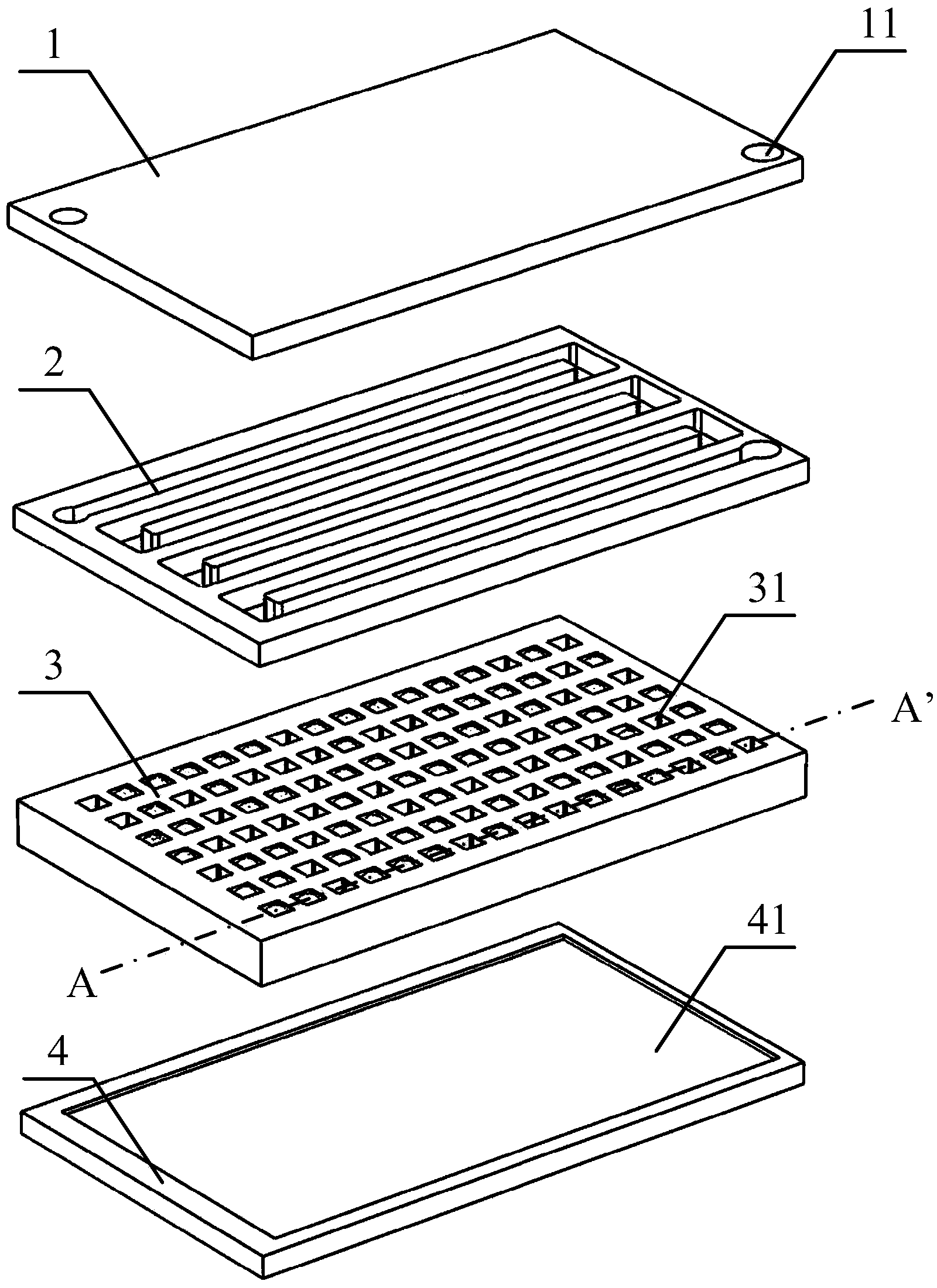
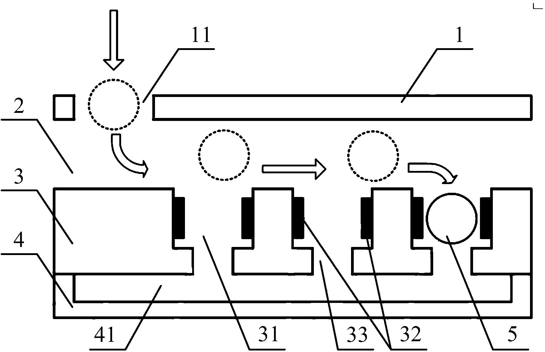
[0072] Transparent top cover: Use 4-inch Pyrex7740 glass sheet (Corning Corporation), cut into rectangular small pieces according to the external dimensions of 2 cm long and 1 cm wide, and punch two holes in specific positions of each small piece with a laser.

[0073] Microfluidic channel: N-type 4-inch silicon wafer is used. After the planar shape of the microfluidic channel is photoetched, ICP dry etching (inductive plasma etching, which uses sulfur hexafluoride and tetrafluoride High-energy plasma of carbon to etch silicon) to create trenches 30 microns deep. Pour the liquid PDMS into the tank, remove it from the mold after it solidifies, cut off the part of the PDMS without the tank, and cut it into rectangular pieces according to the dimensions of 2 cm long and 1 cm wide, thus obtaining microfluidic channels.

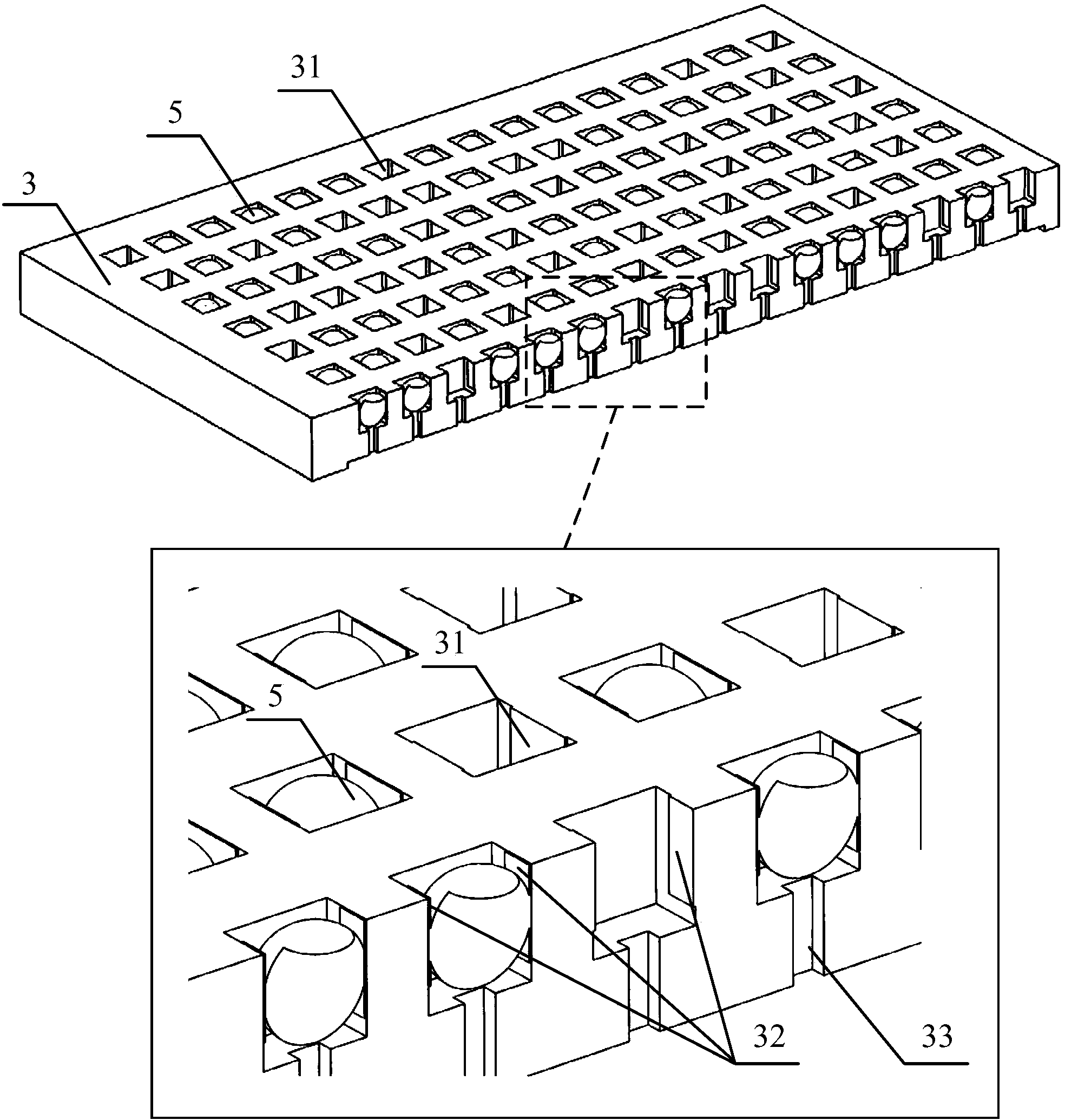
[0074] Substrate with silicon microhole array: N-type 4-inch silicon wafer is used, which is oxidized by wet method to form a 0.5 micron thick oxide layer on the ...

Embodiment 2

[0079] Transparent top cover and microfluidic channel: N-type 4-inch silicon wafer is used. After the planar shape of the microfluidic channel is photoetched, a 30-micron deep groove is etched using ICP dry method. Pour liquid PDMS into the tank, take it out after solidification, and cut it into rectangular pieces according to the dimensions of 2 cm long and 1 cm wide, and use a drill to drill holes at the required positions to form inflow holes and outflow holes, so that A one-piece transparent top cover and microfluidic channels were obtained.

[0080] Substrate with silicon microhole array: N-type 4-inch silicon wafer is used, and chemical vapor deposition (CVD) is used to form a 2 micron thick oxide layer on the surface of the silicon wafer, and microholes are photoetched on the front side of the silicon wafer At the plane position, the micropores are etched 30 microns deep by ICP dry etching. A 0.1-micron-thick chromium metal layer is sputtered on the front side of the s...


PUM

PropertyMeasurementUnit
Widthaaaaaaaaaa
Depthaaaaaaaaaa
Side lengthaaaaaaaaaa

Abstract

The invention relates to a micro-fluidic chip and a micro-fluidic chip system for single cell analysis and a single cell analyzing method. The micro-fluidic chip for single cell analysis comprises a transparent top cover, a microfluid channel, a substrate with a micropore array and a bottom plate with a cavity body, which are sequentially connected from top to bottom in a sealing manner, wherein the transparent top cover is provided with an inflow hole and an outflow hole which are used for communicating the outside and the microfluid channel, the micropore array of the substrate is arranged below the microfluid channel and is communicated with the microfluid channel, each micropore is internally provided with an electrode, each electrode is provided with a cathode and an anode, each micropore can contain a single cell only, the bottom of each micropore is provided with a channel which is communicated with the cavity body of the bottom plate, and the cross section of the channel is smaller than the size of each single cell. With the adoption of the micro-fluidic chip, the micro-fluidic chip system and the single cell analyzing method, the capturing, identifying and disruption processes of each single cell are integrated on one micro-fluidic chip; as a corresponding operation method is provided, the content of each single cell is rapidly acquired and accurately analyzed.

Description

technical field [0001] The invention relates to the technical field of single cell analysis, in particular to a microfluidic chip for single cell analysis integrating the capture, identification and lysis of single cells, as well as a supporting system and a single cell analysis method. Background technique [0002] Obtaining cellular contents is the basis of most molecular biology research, and many modern medical diagnostic methods, such as genome sequencing and proteomic analysis, also require access to cellular contents. The traditional method of obtaining and analyzing cell contents requires a large number of cells, obtains the total content of a certain content (such as nucleic acid or protein), divides the total content by the number of cells, and obtains the number of contents in a single cell . [0003] Obviously, the above method is very imprecise. More importantly, the above method has a necessary premise that the properties of all cells in a single analysis mus...

Claims


Application Information

Patent Timeline
IPC IPC(8): B01L3/00G01N21/64
Inventor 魏泽文胡志远
Owner THE NAT CENT FOR NANOSCI & TECH NCNST OF CHINA
Why Eureka
Try Eureka