Memory and preparation method thereof

A memory and memory technology, applied in the field of organic microelectronic materials, can solve the problems of complex manufacturing process, difficult control of semiconductor materials, high cost, etc., and achieve the effect of high response signal, large industrialization potential and low cost

Active Publication Date: 2014-07-16
SUZHOU UNIV
View PDF3 Cites 3 Cited by
  • Summary
  • Abstract
  • Description
  • Claims
  • Application Information

AI Technical Summary

Problems solved by technology

Although the memory semiconductor memory saves space on the chip and the width of the control valve electrode is not limited by optical lithography, it is expensive, the manufacturing process is complicated, and the semiconductor material is difficult to control.

Method used


Image

  • Memory and preparation method thereof
  • Memory and preparation method thereof
  • Memory and preparation method thereof

Examples


Embodiment 1

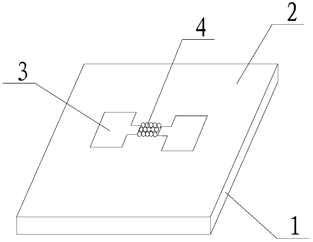
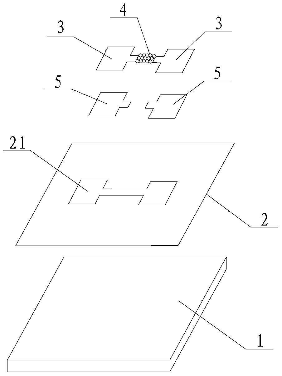
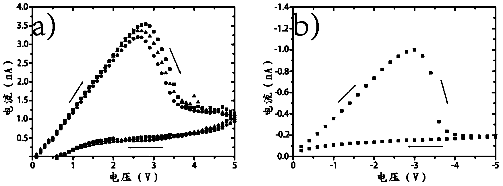
[0030] This embodiment provides a memory storage, such as figure 1 with figure 2 As shown, it mainly includes a semiconductor substrate 1 , an electrode 3 and a thin film layer 4 . Wherein, there are two electrodes 3, which are arranged separately on the upper plane of the semiconductor substrate 1; the thin film layer 4 is also arranged on the upper plane of the semiconductor substrate 1 and connected between the two electrodes 3, and the thin film layer 4 is made of a noble metal coated with a conductive polymer. Nanoparticle composition (i.e. noble metal nanoparticles / conducting polymer composites). Using this composite material to form a thin film layer 4 makes the memory storage device simple in structure, small in size and high in integration, and has great industrialization potential, and the memory storage device has the advantages of low cost, high response signal, and high stability, and has a significant negative differential resistance effect.

[0031] In this ...

Embodiment 2

[0034] This embodiment provides a method for preparing a memory storage device in Embodiment 1, comprising the following steps:

[0035] (a) Spin-coat a layer of photoresist on the semiconductor substrate, heat it at 80-120°C for 1-3 minutes, and carve a cavity on the photoresist;

[0036] (b) Use photolithography or magnetron sputtering technology to first deposit a 3-8nm thick metal chromium layer in the cavity, and then deposit a 15-30nm thick gold layer to form two separated gold electrodes, and then place them in acetone Medium ultrasonic cleaning for about 30 minutes;

[0037] (c) Add 3.6mL of 0.004g / mL chloroauric acid solution to 90.5mL of deionized water, stir and heat to boiling, then add 5mL of 0.0114g / mL sodium citrate solution, and keep boiling for 15min to prepare a 13nm gold nanoparticle solution ;

[0038]Add 25 mL of deionized water, 5 mL of ferric chloride solution with a concentration of 0.125 g / mL, and 50 microliters of pyrrole solution (0.967 g / mL) into ...


PUM

PropertyMeasurementUnit
thicknessaaaaaaaaaa
thicknessaaaaaaaaaa
diameteraaaaaaaaaa

Abstract

The invention relates to a memory and a preparation method thereof. The memory comprises a semi-conductor substrate, two electrodes arranged on the semi-conductor substrate at an interval and a film layer for enabling the two electrodes to be connected, wherein the film layer is composed of precious metal nano particles clad with conducting polymers. The preparation method of the memory comprises the following steps of (a) coating a layer of photoresist on the semi-conductor substrate in a spinning mode, and photoetching a cavity; (b) depositing metal in the cavity to form the two electrodes at an interval; (c) preparing precious metal nano particle / conducting polymer composite materials; (d) dropping the composite materials diluted by deionized water between the two electrodes at an interval. By means of the film layer connected between the two electrodes and composed of the precious metal nano particles clad with the conducting polymers, the memory is simple in structure, small in size, low in cost and high in integration degree and stability and has high response signals.

Description

technical field [0001] The invention belongs to the field of organic microelectronic materials, and in particular relates to a memory storage and a preparation method thereof. Background technique [0002] Devices such as digital cameras, mobile phones, and MP3 players have grown rapidly in the past few years, making consumers' demand for storage media also increase rapidly. Memory memory is an important part of these storage media, which has the characteristics of data non-volatility, power saving, small size, and no mechanical structure. [0003] Conductive polymers and electronic devices based on conductive polymers have been widely studied, which have the advantages of simple fabrication process, low cost, high response signal, and high stability. These electronic devices include light-emitting diodes, field-effect transistors, solar cells, and more. Polypyrrole (PPy) is a common conductive polymer with conjugated chain oxidation and corresponding anion-doped structur...

Claims


Application Information

Patent Timeline
Patent Type & Authority Applications(China)
IPC IPC(8): H01L51/05H01L51/40
CPCH10K71/12H10K10/29
Inventor 江林张军昌
Owner SUZHOU UNIV
Why Eureka
Try Eureka