Organic electroluminescence device and manufacturing method thereof

An electroluminescence device and a luminescence technology, which are applied in organic semiconductor devices, organic semiconductor device materials, electric solid state devices, etc., can solve problems such as poor compatibility, prone to defects, and hole loss

Inactive Publication Date: 2014-07-16
STATE GRID CORP OF CHINA +1
View PDF5 Cites 7 Cited by
  • Summary
  • Abstract
  • Description
  • Claims
  • Application Information

AI Technical Summary

Problems solved by technology

[0004] In traditional light-emitting devices, the material of the hole injection layer is usually metal oxide (such as molybdenum oxide), but at this time the material selection range of the hole injection layer is narrow, and at the same time, the metal oxide has a high absorbance in the visible light range , resulting in loss of sunlight, and the metal oxide is an inorganic substance, which is quite different from the organic material of the hole transport layer. The compatibility between the two is poor on the contact interface. Hole loss and device luminous efficiency reduction

Method used


Image

  • Organic electroluminescence device and manufacturing method thereof
  • Organic electroluminescence device and manufacturing method thereof
  • Organic electroluminescence device and manufacturing method thereof

Examples


Embodiment 1

[0065] An organic electroluminescent device, the preparation method comprising the following steps:

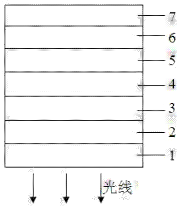
[0066] (1) First set the size to 2×2cm 2 The ITO glass was ultrasonically cleaned with detergent and deionized water for 15 minutes to remove the organic pollutants on the surface. The ITO layer thickness of the ITO glass was 180nm;

[0067] The hole injection layer was prepared by spin coating on ITO glass, and the specific operation was as follows: according to Re 2 o 7 : AIBA: ZnO: polytetrafluoroethylene (PTFE): water with a weight ratio of 30:15:1:2:100, the Re 2 o 7 , AIBA, ZnO, and polytetrafluoroethylene (PTFE) were added into water and mixed evenly to obtain a mixture. The particle size of ZnO was 50nm, and polytetrafluoroethylene (PTFE) was DuPont’s product, model TE3885; The mixture was spin-coated at a high speed, the spin-coating time was 10s, and then dried at 100° C. for 25 minutes to obtain a hole injection layer with a thickness of 80 nm;

[0068] (2) Hol...

Embodiment 2

[0078] An organic electroluminescent device, the preparation method comprising the following steps:

[0079] (1) First set the size to 2×2cm 2 The AZO glass was ultrasonically cleaned with detergent and deionized water for 15 minutes to remove organic pollutants on the surface. The AZO layer thickness of the AZO glass was 80nm;

[0080] The hole injection layer was prepared by spin coating on AZO glass, the specific operation is as follows: according to ReO 2 : AIBI: ZnO: polytetrafluoroethylene (PTFE): ethanol with a weight ratio of 10:2:0.5:0.5:100, the ReO 2 , AIBI, ZnO and polytetrafluoroethylene (PTFE) were added to ethanol and mixed evenly to obtain a mixture. The particle size of ZnO was 20nm, and polytetrafluoroethylene (PTFE) was DuPont’s product, model TE3885; The mixture was spin-coated at a rate of 5 s, and then dried at 200° C. for 10 min to obtain a hole injection layer with a thickness of 100 nm;

[0081] (2) On the hole injection layer, the hole transport la...

Embodiment 3

[0090] An organic electroluminescent device, the preparation method comprising the following steps:

[0091] (1) First set the size to 2×2cm 2 The IZO glass was ultrasonically cleaned with detergent and deionized water for 15 minutes to remove organic pollutants on the surface. The IZO layer thickness of the IZO glass was 100nm;

[0092] The hole injection layer was prepared by spin coating on IZO glass, and the specific operation was as follows: 2 o 3 : V30: ZnO: polytetrafluoroethylene (PTFE): isopropanol with a weight ratio of 60:20:10:5:100, the Re 2 o 3 , V30, ZnO and polytetrafluoroethylene (PTFE) were added to isopropanol and mixed evenly to obtain a mixture. The particle size of ZnO was 200nm, and the polytetrafluoroethylene (PTFE) was DuPont’s product, model TE3885;

[0093] The mixture was spin-coated on the IZO glass at a rate of 6000rpm, the spin-coating time was 30s, and then dried at 50°C for 30min to obtain a hole injection layer with a thickness of 20nm;

...


PUM


Abstract

The invention provides an organic electroluminescence device and a manufacturing method thereof. The organic electroluminescence device comprises a conductive anode substrate, a hole injection layer, a hole transmission layer, a light emitting layer, an electron transmission layer, an electron injection layer and a cathode which are stacked sequentially, wherein the hole injection layer is made of a mixture of rhenium oxide and zinc oxide, the hole injection layer further contains the binder polytetrafluoroethylene, the hole injection layer is of a nanometer netty structure, and the bore diameter of the nanometer netty structure is 100 nm - 150 nm. According to the organic electroluminescence device, the hole transmission layer is manufactured through mixture of rhenium oxide, azo substances, zinc oxide and polytetrafluoroethylene, the binder polytetrafluoroethylene enables the cohesiveness between the hole injection layer and adjacent layers to be improved, decomposition of the azo substances enables the nanometer netty structure of the hole injection layer to be formed, the hole transmission rate and the photoelectric conversion efficiency of the device can be improved, the manufacturing method is simple, and application prospects are good.

Description

technical field [0001] The invention relates to the field of organic electroluminescence, in particular to an organic electroluminescence device and a preparation method thereof. Background technique [0002] In 1987, C.W.Tang and Van Slyke of Eastman Kodak Company in the United States reported a breakthrough in organic electroluminescence research, using ultra-thin film technology to prepare a high-brightness, high-efficiency double-layer organic electroluminescent device (OLED). In this double-layer structure device, the brightness reaches 1000cd / m at 10V 2 , its luminous efficiency is 1.51lm / W, and its lifespan is more than 100 hours. [0003] The luminescent principle of OLED is based on the action of an external electric field, electrons are injected from the cathode to the lowest unoccupied molecular orbital (LUMO) of organic matter, and holes are injected from the anode to the highest occupied orbital (HOMO) of organic matter. The light-emitting layers meet, recombi...

Claims


Application Information

Patent Timeline
Patent Type & Authority Applications(China)
IPC IPC(8): H01L51/50H01L51/56
CPCH10K50/17H10K50/15H10K2102/00H10K71/00
Inventor 周明杰王平黄辉陈吉星
Owner STATE GRID CORP OF CHINA
Why Eureka
Try Eureka