
Method for preparing doping porous silicon ball
A technology of porous silicon and silicon spheres, applied in the fields of nanostructure manufacturing, nanotechnology, nanotechnology, etc., to achieve uniform morphology, accelerated reaction process, and good industrial value.
- Summary
- Abstract
- Description
- Claims
- Application Information
AI Technical Summary
Problems solved by technology
Method used
Image

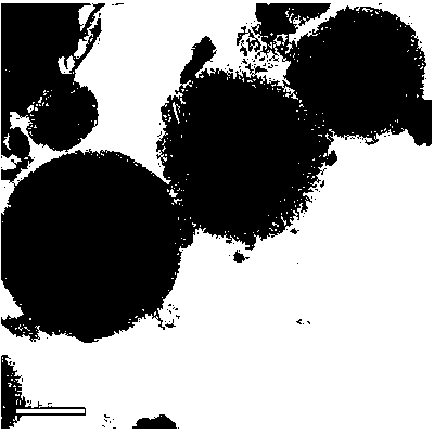
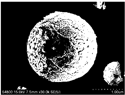
Examples
Embodiment 1
[0036] This embodiment provides a method for preparing nanoporous silicon using doped silicon spheres. When using doped silicon spheres as a raw material, chemical etching is used to prepare nanoporous silicon. The specific steps are as follows:
[0037] 1) The boron doping concentration is selected to be 5.09×10 19 atoms / cm 3 (Conductivity 0.002~0.0025Ω·cm) P-type single crystal silicon master alloy is used as raw material, processed by pulse discharge method, processing parameters are: open circuit voltage 100V; peak current 5A; pulse width 50μs; duty ratio 1:2, The working fluid is deionized water, and the electrodes are copper electrodes. Process and collect doped silicon spheres, the particle size range of silicon spheres is 0.1-2 μm, the size is concentrated at 1 μm, and the concentration is greater than 90%.
[0038] 2) Measure 10g of silicon spheres as the base material;
[0039] 3) Clean the surface of the silicon ball with a chemical solution, the solution is 5% h...
Embodiment 2
[0050] This embodiment provides a method for preparing nanoporous silicon using doped silicon spheres. When using doped silicon spheres as a raw material, chemical etching is used to prepare nanoporous silicon. The specific steps are as follows:
[0051] 1) The phosphorus doping concentration is selected as 2.02×10 15 atoms / cm 3 N-type single crystal silicon ingot (conductivity 1~3Ω·cm) is used as raw material, processed by pulse discharge method, processing parameters are: open circuit voltage 150V; peak current 10A; pulse width 100μs; duty ratio 1:5, working fluid For deionized water, the electrode is a copper electrode. Process and collect doped silicon spheres, the particle size range of silicon spheres is 1-10 μm, the size is concentrated at 5 μm, and the concentration is greater than 90%.
[0052] 2) Measure 10g of silicon spheres as the base material;
[0053] 3) Clean the surface of the silicon ball with a chemical solution, the solution is 10% hydrofluoric acid sol...
PUM
 Abstract
Description
Claims
Application Information