Grid-controlled vertical double-diffusion metal-oxide semiconductor field effect transistor

A gate oxide layer and gate technology, which is applied to semiconductor devices, electrical components, circuits, etc., can solve the problems of large cell size, insufficient cell density, and high power consumption.

Active Publication Date: 2014-08-27
XIDIAN UNIV
View PDF4 Cites 2 Cited by
  • Summary
  • Abstract
  • Description
  • Claims
  • Application Information

AI Technical Summary

Problems solved by technology

[0007] In order to solve the problems in the prior art, such as large power consumption caused by the inability to reduce the series resistance of the JFET area of ​​the transistor, large cell size and i

Method used


Image

  • Grid-controlled vertical double-diffusion metal-oxide semiconductor field effect transistor
  • Grid-controlled vertical double-diffusion metal-oxide semiconductor field effect transistor
  • Grid-controlled vertical double-diffusion metal-oxide semiconductor field effect transistor

Examples


Embodiment Construction

[0027] The present invention will be further described in detail below with reference to the accompanying drawings and specific embodiments.

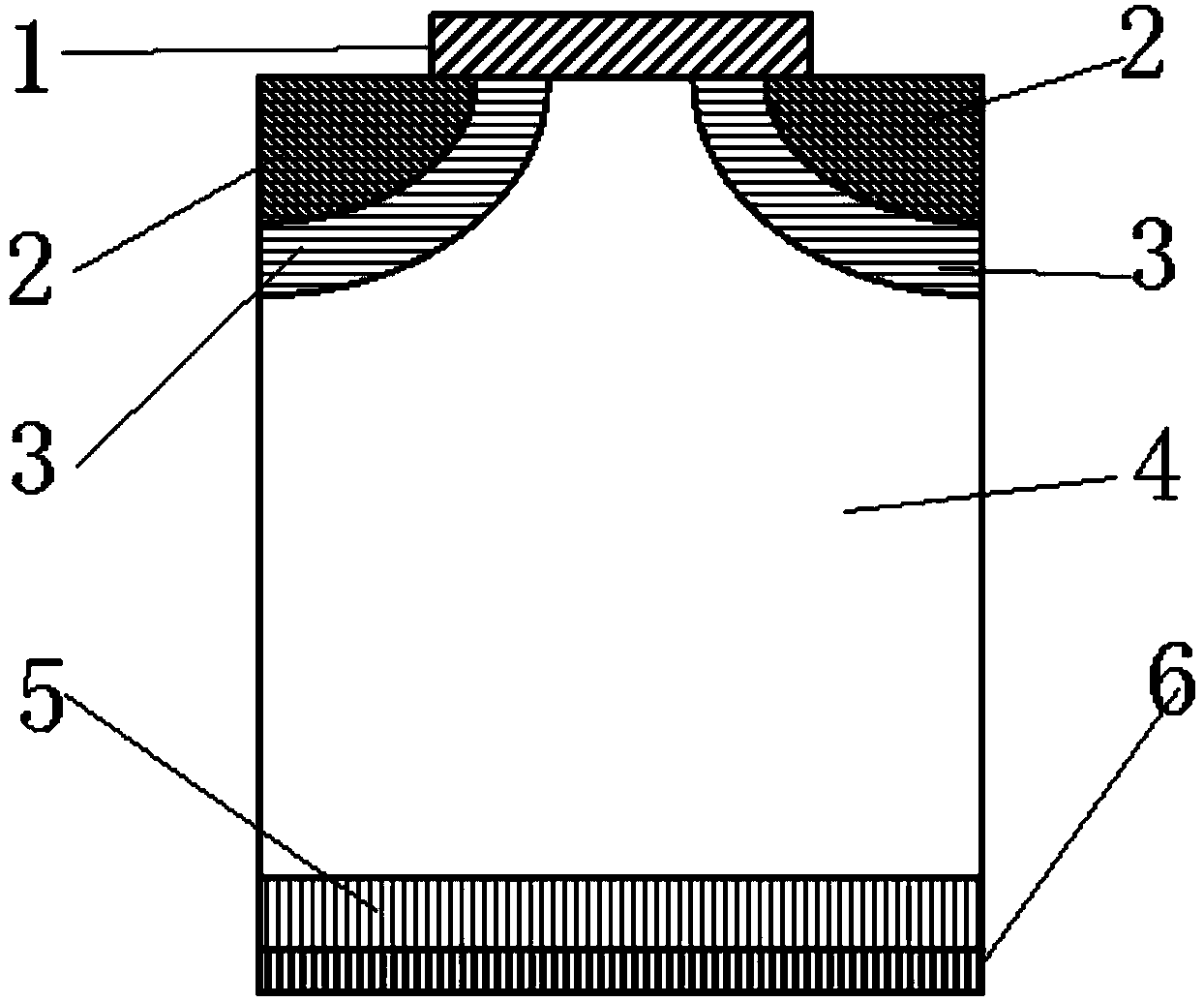
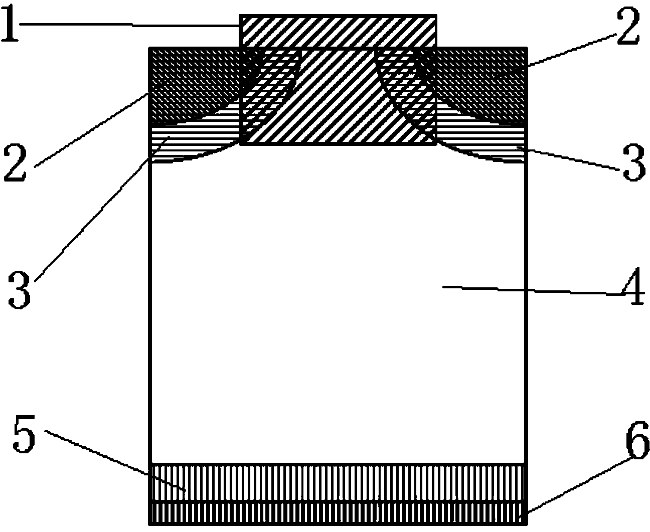
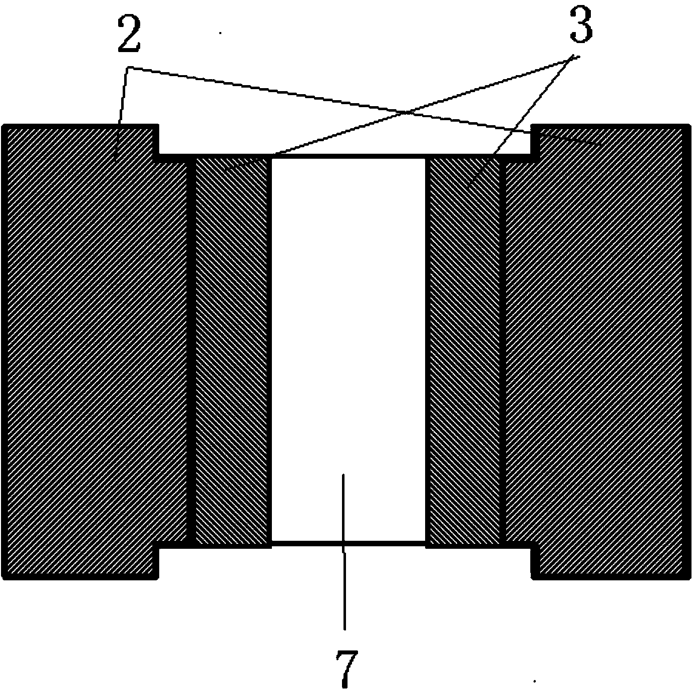
[0028] Take N-channel VDMOS device as an example, such as figure 2 As shown, it includes gate 1, N+ source region 2, P-type base region 3, N-drift region 4, N+ substrate 5, drain 6, and its gate 1 (across the gate oxide layer) covers the transistor. The channel region and the JFET region are from the top surface and the front and rear sides. During forward conduction, under the action of the gate voltage, the extended gate electrode makes both the channel region and the JFET region generate a charge accumulation layer, which can significantly reduce the on-resistance and increase the output current. Moreover, due to the ability of the folded gate to control the charge of the JFET region, the punch-through problem caused by the reduced size of the JFET region can be avoided, thereby promoting the charge sharing effect of the cells, opt...


PUM


Abstract

The invention discloses a grid-controlled vertical double-diffusion metal-oxide semiconductor field effect transistor. A channel region and a JFET region of the transistor are wrapped in gate electrodes from the upper surface, the front side face and the rear side face, so that when the transistor is powered on in the forward direction, majority carrier accumulation layers are formed on the channel region of a device and the JFET region of the device respectively through the expanded grid electrodes, the on resistance can be decreased remarkably, and the output current can be increased. Moreover, due to the capability of folding grids for controlling electric charges of the JFET region, the punch through problem caused by the shrinkage of the size of the JFET region can be avoided, so that the charge sharing effect of cellular cells is promoted, vertical electric field distribution is optimized, and the puncture voltage of the device is increased. Besides, cellular miniaturization is facilitated due to the shrinkage of the size of the JFET region, cellular density is increased, and thus the larger current can be obtained.

Description

technical field [0001] The present invention relates to the technical field of semiconductor devices, in particular to a vertical double-diffused metal-oxide semiconductor field effect transistor. Background technique [0002] Power MOS field effect transistor is a new generation of semiconductor power switching device developed on the basis of MOS integrated circuit technology. It has made great progress in the past two decades. It started from LDMOS structure and has experienced the evolution of VVMOS, VUMOS, VDMOS, EXTFET and other structures. , VDMOS structure is still dominated at present. Vertical double-diffused metal oxide semiconductor (VDMOS) devices have a series of unique features such as high input impedance, fast switching speed, high operating frequency, voltage control, and good thermal stability. Steady-state power supply, high-frequency heating, computer interface circuits and power amplifiers have been widely used. [0003] To fulfill the function of a po...

Claims


Application Information

Patent Timeline
IPC IPC(8): H01L29/78H01L29/423
CPCH01L29/4236H01L29/7813
Inventor 段宝兴袁嵩杨银堂郭海君
Owner XIDIAN UNIV
Why Eureka
Try Eureka